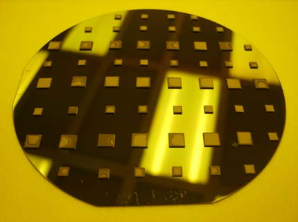
We report a batch-mode fabrication technology for integration of bulk piezoelectric materials into MEMS devices, and test results of high-performance out-of-plane piezoelectric actuators fabricated with this technology. Low-temperature (200℃), reliable AuIn and Parylene bonding of PZT wafers/dies on Si wafers is achieved, and lapping is used to obtain <10μm PZT films. Conservation of the piezoelectric properties is confirmed with a hysteresis measurement. Additionally, square and circular shaped PZT diaphragms with 4mm×4mm, 2mm×2mm, and 1mm×1mm sizes operating in the d31-mode are fabricated with a 2-mask fabrication process. Greater than 12 μm peak-to-peak deflection is obtained by actuation of a 1mm2 diaphragm at resonance (110.9kHz) with a power consumption of <7mW.
Bulk piezoelectric ceramics, unlike deposited piezoelectric thin films (<few µm), provide greater electromechanical force, structural strength, and charge capacity, which are highly desirable in many MEMS applications including high-force actuators, harshenvironmental sensors, and micro-power scavengers. Previous studies for integration of bulk ceramics in MEMS focused on bonding by surface activation , hydrophilic conditioning, epoxy-resin, Cytop, AuSn, or InSn. However, these manufacturing techniques have faced significant challenges such as a non-patternable bond layer, low bond strength due to high stress and voids in the bond layer, or out-diffusion of lead and repolarization issues due to high temperature processing. In this study, we have developed low-temperature, fluxless, patternable, and reliable AuIn (conductive) and Parylene (non-conductive) bonding of bulk PZT-5A on Si wafers, both in die and wafer level (70mm×70mm), and have demonstrated that bonded PZT wafer/pieces can be thinned down at wafer-level to less than 10μm.
Bonded PZT-5A samples do not require repolarization, since the bonding temperature is around half of the Curie temperature (350℃). The bond shear strength is measured and summarized in Table 1 for both AuIn and Parylene bonded samples. During shear tests, more than 50% of the AuIn samples failed due to cracking that occurred in the PZT or the Si, which indicates that the bond layer has greater strength than the bonded material itself. After bonding, ferroelectric properties are confirmed by measuring the remnant polarization (37.7ȝ C/cm2 ) and the coercive field (16.8kV/cm) (Fig.4a).
Actuated displacements of fabricated diaphragms are measured using a laser vibrometer. In order to confirm that the piezoelectric properties of the bulk material are fully conserved, measured out-of-resonance displacement of a diaphragm is compared with its FEA simulation at static actuation (Fig.8). The simulation results are represented with the shaded area, in order to account for +/g 0.5μm variation in PZT and AuIn thickness values, due to the rough interface between these layers.

Fig1
Bulk piezoelectric ceramics, unlike deposited piezoelectric thin films (<few µm), provide greater electromechanical force, structural strength, and charge capacity, which are highly desirable in many MEMS applications including high-force actuators, harshenvironmental sensors, and micro-power scavengers. Previous studies for integration of bulk ceramics in MEMS focused on bonding by surface activation , hydrophilic conditioning , epoxy-resin , Cytop , AuSn , or InSn. However, these manufacturing techniques have faced significant challenges such as a non-patternable bond layer, low bond strength due to high stress and voids in the bond layer, or out-diffusion of lead and repolarization issues due to high temperature processing. In this study, we have developed low-temperature, fluxless, patternable, and reliable AuIn (conductive) and Parylene (non-conductive) bonding of bulk PZT-5A on Si wafers, both in die and wafer level (70mm×70mm), and have demonstrated that bonded PZT wafer/pieces can be thinned down at wafer-level to less than 10μm.