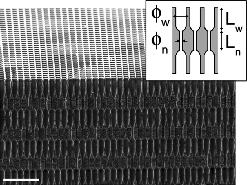
All these methods produce one single layer of silicon at a time. If a second one is needed, the process must be repeated from the beginning. Here, we show how to obtain, from a single silicon wafer and on a single fabrication step, multiple “epi-free” c-Silicon thin layers with controlled thickness or, as we call it, a “millefeuille” of crystalline silicon. The methodology is also based on the annealing of porous silicon structures. In such process, the evolution of the pores during annealing is governed by surface diffusion as described by the Mullin’s equation.Recently, sine generated curves (i.e., curves whose curvature is a sine function of the arc-length parameter), which have been used in the past to describe river meanders, have been found to describe the evolution of high aspect ratio surfaces mediated by surface diffusion. A detailed inspection of these results suggests that, by accurately controlling the profifile of the pores, it should be possible to obtain multiple crystalline layers separated by voids. Hereafter, we show how, through a precise in-depth modulation of pore diameter, both the number of layers and their thickness can be controlled.
In this way, we achieve both full wafer area and layer thickness fabrication control. In principle, the whole wafer can be sliced in a single step following this process, being the resulting number of layers only determined by wafer initial thickness and the thicknesses of the layers. Fig. 1(b) shows a Scanning Electron Microscope (SEM) image of a final sample before exfoliation where the formation of independent thin layers over the silicon bulk is clearly observed. The given image reveals the fabrication of 10 layers (not all clearly visible) with thicknesses around 6 lm. The ten thin films reported in the figure were produced in 3 h etch (120 lm depth pores).
After layer formation, silicon thin films are tapeexfoliated from the substrate to characterize their structural properties. Some exfoliated films are shown in Fig. 6. Thinner layers, around 1–2 lm, present brown color (Fig. 6(a)) due to optical transmission properties of silicon and thicker layers present the typical gray-silicon color. Additionally, in Fig. 6(b), we present a set of three samples exfoliated from the same original silicon “millefeuille.” Films have been sticked to a glass slide for characterization. We expect, from the properties of the presented technique, that the formed multiple layers should preserve the crystallographic orientation of the bulk, which is important for applications. We have confirmed it by X-ray texture analysis on different final layers, with and without pores inside. A single crystallographic peak is found at 69.3 marking the h400i silicon orientation, as it was in bulk, in all analyzed layers. The same results have been obtained in all samples. We have also characterized the roughness of the obtained layers by interferometry. Thinner layers, around 1–2 lm, present an average roughness of 100–130 nm, while the average roughness of the thicker layers is in between 250 and 300 nm. Although the crystal quality of the reported thin films is good as stated in Ref. 18, stacking fault density and dislocations among the structure are currently under investigation.

Fig1
The presented discussion is depicted in Fig. 5, where SEM images of different fifinal structures are presented. Solid layer formation is observed in image (a). A total number of 3 layers with average thickness of 6.5 lm, plus a very thin top one, have been fabricated. Larger number of layers is shown in image (b), where the presence of trapped spheres is observed due to the larger /n value. Image (c) shows the result of a low-amplitude pore modulation, as previously discussed, leading to the formation of a fifirst solid thin layer followed by a highly porous layer with nearly 40 lm thickness. Finally, SEM image (d) shows alternate layers with thicknesses of 4 and 8 lm. An important feature of the presented fabrication technique is that the length Ln can be independently controlled, which makes it possible to obtain, from a single initial wafer, different layers with different thicknesses.
In conclusion, multiple silicon layers from a single wafer in a controlled way have been produced. We have shown that, by choosing optimized diameter modulation of the pores, we are able to obtain different numbers of layers whose thickness can also be varied in a large extent. In this proof of concept, samples’ area has been limited to 15 mm diameter for convenience, although the technology is scalable to full wafer scale. Further work is needed in order to in-depth explore the possibilities and limitations of the proposed technique.