Silicon photonics is becoming a mainstream data-transmission solution for next-generation data centers, highperformance computers, and many emerging applications. The inefficiency of light emission in silicon still requires the integration of a III/V laser chip or optical gain materials onto a silicon substrate. A number of integration approaches, including flip-chip bonding, molecule or polymer wafer bonding, and monolithic III/V epitaxy, have been extensively explored in the past decade. Here, we demonstrate a novel photonic integration method of epitaxial regrowth of III/V on a III/V-on-SOI bonding template to realize heterogeneous lasers on silicon. This method decouples the correlated root causes, i.e., lattice, thermal, and domain mismatches, which are all responsible for a large number of detrimental dislocations in the heteroepitaxy process. The grown multi-quantum well vertical p–i–n diode laser structure shows a significantly low dislocation density of 9.5 × 104 cm−2 , two orders of magnitude lower than the state-of-the-art conventional monolithic growth on Si. This low dislocation density would eliminate defect-induced laser lifetime concerns for practical applications. The fabricated lasers show room-temperature pulsed and continuous-wave lasing at 1.31 μm, with a minimal threshold current density of 813 A/cm2 . This generic concept can be applied to other material systems to provide higher integration density, more functionalities and lower total cost for photonics as well as microelectronics, MEMS, and many other applications.
In this paper, we demonstrate our recent development9 of a novel platform to integrate III/V materials into SOI substrates. It combines the advantages of monolithic growth and wafer bonding approaches, aiming to provide a low-dislocation-density, low-cost wafer-scale integration scheme. A combination of epitaxial growth and wafer bonding has been reported for lateral injection membrane lasers and double-heterostructure lasers13. However, the former requires a relatively complex and unconventional process to make p- and n-doping regions and to form a lateral p–i–n diode structure through an extra regrowth step. This unique process has enabled very impressive laser performance, but is not readily available in most commercial epitaxial growers. The latter uses a bonded thick InP growth template and buffer layer on a bulk Si substrate, which is challenging to integrate with other Si photonic circuits on the same chip, as discussed before. In this work, a standard ~2-μm-thick InGaAsPbased multi-quantum well (MQW) laser structure is epitaxially grown on a bonded InP-on-SOI template with signifificantly low threading-dislocation density (TDD), measured to be <1 × 105 cm−2 , despite the impact of thermal mismatch. Fabricated Fabry–Perot (FP) lasers show continuous wave (cw) and pulsed lasing up to 40 °C and a good threshold current and output power. Based on the excellent material quality of the regrown MQW and proof-of-concept laser performance, a number of merits of this demonstrated bonding plus epitaxy approach are discussed. The low dislocation density achieved in this integration approach would eliminate defect-induced lifetime concerns for practical applications. This bonding plus epitaxy idea is generically applicable for the integration of many more dissimilar materials. In particular, to compare with the presently popular III/V-to-Si wafer bonding approach, it enables III/V epitaxy on a much larger wafer scale at a lower epitaxy cost. Multiple sequential regrowths on the same bonded template allow integration of more than one III–V epitaxial structure for more advanced photonic integration, similar to bonding different III–V dies on the same Si wafer. However, our approach can lead to more intimate integration and benefifits from a simpler single-bonding step.
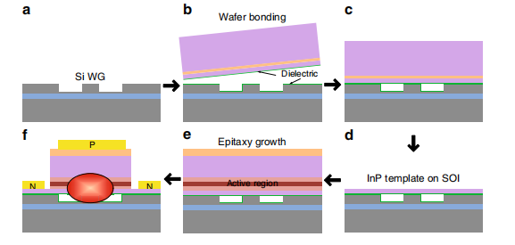
Figure 1 shows a schematic of the process of our integration scheme. First, Si waveguides and some bondingfacilitating vertical outgassing structures14 were created in the SOI substrate (Fig. 1a). Second, an InP substrate wafer topped with a n-InP template layer and InGaAs etch-stop layer was bonded to the SOI wafer by direct wafer bonding (Fig. 1b, c). Upon selectively removing the InP substrate and InGaAs etch-stop layer to expose the n-InP template layer (Fig. 1d), the wafer-bonded InP-on-SOI substrate was loaded into a metal–organic chemical vapor deposition (MOCVD) chamber for epitaxial growth to form a conventional vertical p–i–n diode laser structure (Fig. 1e), similar to that previously reported for full III/V epitaxial stack bonding15. Finally, the heterogeneous wafer underwent a standard III/V process to fabricate laser devices (Fig. 1f). The bonded template was introduced to eliminate lattice and polarity mismatches between the Si and III/V material; thus, the thick intermediate buffer layer typically required in conventional III/V-on-Si direct epitaxy is not necessary. In addition, the n-InP template is only 150 -nm thick, similar to that previously reported in the full III/V stack bonding design. This enables facile light coupling from grown III/V active layers to Si waveguides. Figure 2a shows the heterogeneous wafer with the transferred n-InP template and the wafer under device fabrication after epitaxy. The heterogeneous wafer exhibited good yield and robustness after bonding annealing at 300 ° C, epitaxy growth at 600 °C, and post-epitaxy device fabrication. Figure 2b shows the epitaxy structure grown on the bonded template, similar to well-demonstrated heterogeneous laser structures16 with low-loss evanescent coupling to the Si photonic circuits. The MQW is designed for light emission at 1.31 μm. The total epitaxy thickness is ~2 μm. An identical structure was grown on a witness InP wafer in the same growth chamber.

Fig1
The main advantage of conducting epitaxy on the bonded template is eliminating two out of three major dislocation root causes: lattice and polarity mismatches between the substrate (e.g., Si) and the function material (e.g., InP-based III/V) from epitaxial growth. The thermal mismatch between the substrate and template material would still cause dislocations in the regrown materials, but it is measured to be at a significantly low level. According to the aging tests of InAs QD lasers on Si near room temperature , a reduction in the TDD from 108 cm−2 to 106 cm−2 can extend the laser lifetime from a few months to over 100 years. It is reasonable to expect that lasers from the regrowth on the bonded template with even lower dislocation density would eliminate the defectinduced lifetime concerns for all practical applications.