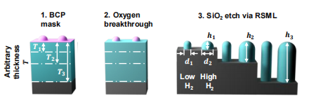
Silicon nanostructuring imparts unique material properties including antireflectivity, antifogging, anti-icing, self-cleaning, and/or antimicrobial activity. To tune these properties however, a good control over features size and shape is essential. Here, a versatile fabrication process is presented to achieve tailored silicon nanostructures (thin/thick pillars, sharp/truncated/re-entrant cones), of pitch down to ~50 nm, and high-aspect ratio (>10). The approach relies on pre-assembled block copolymer (BCP) micelles and their direct transfer into a glass hard mask of an arbitrary thickness, now enabled by our recently reported regenerative secondary mask lithography. During this pattern transfer, not only the mask diameter can be decreased but also uniquely increased; constituting the first method to achieve such tunability without necessitating a different molecular weight BCP. Consequently, the hard mask modulation (height, diameter) advances the flexibility in attainable inter-pillar spacing, aspect ratios, and reentrant profiles (=glass on silicon). Combined with adjusted silicon etch conditions, the morphology of nanopatterns can be highly customized. The process control and scalability enable uniform patterning of a 6-inch wafer which is verified through cross-wafer excellent antireflectivity (<5%) and water-repellency (advancing contact angle 158°; hysteresis 1°). It is envisioned the implementation of this approach to silicon nanostructuring to be far-reaching, facilitating fundamental studies and targeting applications spanning solar panels, antifogging/antibacterial surfaces, sensing, amongst many others.
Nanopatterning of silicon to afford superior functionality and performance has become commonplace, with demonstrations spanning solar cells, energy storage, thermoelectrics, sensors, antibacterial and special wetting surfaces. To elicit the desired and new functionalities however, it is critical to control both the morphology and dimensions of nanofeatures while accommodating a continuous demand for higher resolution and aspect ratio (AR). Such requirements concurrent with method scalability, reliability, and compatibility with existing manufacturing processes are not trivial to achieve, bringing a necessity to advance nanofabrication techniques. In this regard, pattern transfer using block copolymers (BCPs) has been investigated due to their low cost, morphological diversity and proficiency in high resolution patterning (5-200 nm); overcoming the limitations posed by photolithography and electron beam lithography, for instance.
Nonetheless, BCP lithography holds its own challenges related either to feasibility of morphology control or insufficient etching contrast. To overcome the former, substrate preparation (neutral brush layer), thermal/solvent annealing, and development steps have been adapted. Here, conditions need to be carefully chosen, particularly during annealing to prevent de-wetting or undesired morphology formation. This increases the complexity and cost of the fabrication, which constitutes a potential challenge for implementation in industry. Furthermore, control over pitch demands individual optimization for BCPs of different molecular weight Mw, limiting flexibility. Recently, an alternative BCP micelle lithography process was presented whereby preassembled solution-phase micelles of poly(styrene – block – 2-vinylpyridine) (PS-b-P2VP) were directly spin-coated onto a substrate, yielding micellar bumps which act as a topographic contrast. This route negates the aforementioned steps, whilst enabling reduction of mask diameter, pitch fine-control through spin speed variation, and coarse-control through choosing a different Mw BCP (without individual optimization).

Fig1
The pattern transfer into the Si layer (Figure 1; step 4) is governed by a combination of the SiO2 mask morphology (h/d), and the Si etch conditions. Here, we use Cl2 plasma, with a characteristic etching selectivity >5, dependent on the coil/platen power, Cl2 flow, and pressure. Through manipulation of the glass and Si etching, we realize high AR nanostructures with sophisticated sidewall profiles, including nanopillars, nanocones with truncated or sharp tips, re-entrant structures and nanopyramids, all of which are discussed separately in the following sub-sections.
As in glass etching, a facile route for high aspect ratio silicon nanostructure generation has been absent, due to the lack of BCP mask durability. However, through RSML, we increase the AR of the SiO2 hard mask, and overcome this issue. Figure 3b shows three hard masks of increasing h (100-350 nm), and the corresponding Si nanostructures etched under the same conditions. All structures are etched to the point of mask consumption to yield the highest AR (AR>10, Figure 3,vi), however this can introduce distortion. To avoid this therefore, etching should be stopped just prior to hard mask depletion, and followed by post-processing hard mask removal (e.g., HF treatment). Important to note, is that high AR hard masks, such as that shown in Figure 3b,iii, can lead to bowing as a result of the mask weight and the AR of the Si structures. Nonetheless, the resulting Si nanograss (Figure 3b,vi) are likely to bring antireflective properties or may be effective in antibacterial performance.
上一篇: 用于高性能柔性电子产品的超薄芯片