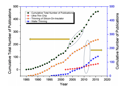
The technology readiness to obtain devices down to nanoscale dimensions and the possibility to exponentially scale the device densities up to billions of devices per mm2 , makes silicon based microelectronics a good candidate for addressing immediate high-performance needs in flexible electronics. For this the first issue that need to be overcome is the lack of flexibility (and hence conformability) of silicon wafers. This has been achieved by thinning the wafers down to <50 µm using a range of technologies, which are discussed here. Silicon chips from such thinned wafers, or ultra-thin chips (UTCs), are ideal for highperformance flexible electronics as they are physically bendable and have stable electronic response for particular bending state.13 The excellent form factor of UTCs make their integration on flexible substrates better than the conventional thick chips. Further, due to reduced package volume and lower parasitic capacitance, the UTCs have better high-frequency performances and lower power consumption. With these features UTCs can underpin advances in areas such as sensing, computing, data storage, and energy (Fig. 1) and several emerging applications (e.g., robotics, wearable systems, m-Health, smart cities and Internet of Things etc.) they will enable.
Given the wide scope of UTCs, a comprehensive review of various technological and applied aspects will complement several other reviews that have mainly focussed on organic semiconductors and their processing techniques such as printing or vacuum deposition etc. A few review articles have also discussed layer transfer processes and thin film silicon for solar cells. Related to UTCs, only a few review articles have been published and they have covered limited areas such as wafer thinning methods such as back grinding and integration on flexible substrate using stretchable interconnects. The analysis of UTCs covering topics such as changes in electricalmechanical-optical-thermal properties, packaging, and stressinduced response variations, and comparison of various thinning methods has not been reported thus far. The in-depth analysis presented in this paper fills the above gaps in the literature and provide a complete overview of the research related to UTCs.
The physical dimensions could influence the material properties and carrier transport mechanism and therefore could affect the performance of electronics devices. Compared to their bulk counterparts, the UTCs exhibit different behavior in terms of mechanical flexibility, optical transmittance, and carrier surface mobility (e.g., upon experiencing stress) etc. These variations can be challenging to handle, for example when one attempts to apply on UTCs the methods and designs developed for conventional bulk silicon. At the same time, such variations also offer multiple new opportunities, which are otherwise difficult with bulk silicon. For example, Si starts to become optically transparent for thicknesses below 10 µm—starting in the red region and progressing towards blue region as the wafer gets thinner. Such thinning led variations in optical transparency of Si could be exploited to improve photodetectors and solar cells etc., as explained later in this section. An extensive analysis of variations in properties with respect to thickness has not been reported and this section should fill the gap in literature.
The thinning process impacts the mechanical properties of thinned electronic substrate. For example, during thinning by back grinding, the sub-surface damage (SSD) and deep cracks in Si result in poor bendability and eventually lead to early breakage of UTCs. Likewise, the etch pits and hillocks produced during thinning by wet etching could lead to localized stress and can decrease the breaking strength of Si. The localised stress or stress distribution at different locations in UTCs are typically studied with Finite Element Analysis29 and Micro-Raman Spectroscopy. The FEM analysis can provide an estimate of the residual stress at critical position like hinge and centre and the shift in Raman peak could provide deep insight into localised mechanical stresses.

Fig1
MOSFETs show increase in mobility with increase in bending stress. In n-type MOSFETs, this behaviour is independent of the direction of bending, but variations in the response of p-type MOSFETs is direction dependent. The models in these works have taken into account the process strategies, dimensions of the structure (active Si, dielectric, metal thicknesses, etc.), initial substrate (e.g., Si, SOI, UTSOI, ETSOI etc.), mechanical strain etc. The stressed induced changes could lead to signifificant deviations in the response of device and circuits from their specified values, as can be oberved from Table 2, where bending induced changes in device and circuit parameters are reported. For complex circuit design in flexible electronics and to predict their response under different bending condition precisely, it is necessary to understand these variations and implement predictive models in electronics design tools. The variations in device response could be reduced by using suitable compensation techniques in the layout. On other hand, these changes in the device parameters could also be seen as the signature for a particular bending state and therefore could be used to predict or sense the state/shape of bending.
A wide range of technologies have been explored for realizing UTCs and a detailed discussion about some of are given in a few review articles. For the sake of completeness, the technologies involving either bulk Si wafer or SOI wafer are briefly discussed in this section. Figure 4 also gives a summary of these technologies, classified based on the fabrication stage at which the thinning is carried out. For example, when the thinning is carried out after the fabrication of electronic devices it is termed as post-processing, and when wafer undergoes some processing before the device fabrication then it is termed as pre-processing. Generally, the thinning is carried out after the device fabrication is completed. Following the discussion in previous section, the choice of technological approach to realize UTC requires careful consideration.