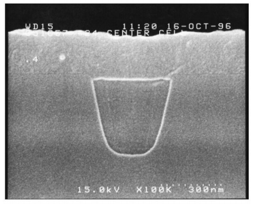
As device geometrics have continued to shrink and circuit complexity has continued to grow, the device isolation has become a major factor limiting the circuit density. The traditional local oxidation of silicon (LOCOS) has a limitation for sub-half micron generation due to the lateral encroachment of ®eld oxide upon the device active areas, ®eld oxide thinning in sub-micron regions of exposed silicon, nonplanarity, and stress-induced silicon defects. In order to increase the device package density for high performance VLSI/ULSI technology, the shallow trench isolation (STI) process becomes attractive. STI improves the isolation between devices where compared to conventional LOCOS-type isolation techniques. Although, the CMP process is well recognized as a powerful method for global planarization, several issues associated with CMP including dishing, oxide remaining above nitride and postCMP cleaning have to be resolved before STI can be fully replace LOCOS.
During the CMP process, the wafer surface is contaminated with silica particles and metallic impurities. These defects can introduce many crystal defects in Si wafers during furnace processing, since the planarization of STI is carried out at the front-end-of-line. However, the removal of the defects is dif®cult because the poly-Si or Si substrate surface is hydrophobic and SiO2 surface is hydrophilic and the surface of silicon nitride is easily charged up. In this paper, we introduce a modi®ed multi-chemical spray cleaning process for post STI CMP cleaning process to assist in the removal of the defects and metallic impurities.
In this paper, all of the data presented was obtained from testing 200-mm wafers. The STI ®ll was deposited by the sub-atmospheric chemical vapor deposition (SACVD, 450 Torr) technique which was a TEOS base system. Figs. 1 and 2 show the STI process and trench scheme. First of all, the LPCVD nitride deposited 150 , 200 nm and after pattern de®ne and trench etching, the STI was formed. The depth of the trench is 350 nm and trench density is 36%. The SACVD was deposited 600 nm on pattern wafers and was subsequently polished 200 nm.
The polishing process was performed on Applied Mirra polisher multi-head, multi-platen system. Table 1 shows the detail parameters of STI CMP in the Applied Mirra polisher. The polishing pads were IC1000/Suba-IV perforated pads made by Rodel. The KOH-based colloidal fumed silica slurry (SS-12) from Cabot was used for the oxide CMP. The modi®ed multi-chemicals spray cleaner used in this study had a standard FSI MERCURY spray cleaner and a SCREEN AS-2000 Post-CMP processor with PVA brush. The APM (ammonia/peroxide mix) and HPM (hydrochloric/peroxide mix) was heated before being delivered to the chamber in the FSI system. Most of the cleaning recipe was modi®ed and followed the procedure formulated by Kern and Puotieu at RCA, which is often referred to as the RCA method. Table 2 lists the clean recipes used in this study.

Fig1
All of the polished wafers were cleaned in the spray processor using different chemicals. The combined effects of APM, HPM and dilute HF scrubber were evaluated on the surface of wafers. Fig. 3 shows the trend chart of particles removed for different cleaning chemical ratios of NH4OH in the APM. From the results, the particle removal ef®ciency is very sensitive to the NH4OH content in the APM. In order to improve particle removal results, the combined effect of APM, dilute HF scrubbing and HPM was also evaluated. In order to eliminate the possibility of poor surface roughness after a HF dip, different dilute HF treatments were also examined. Table 3 lists the results for different combined cleaning recipes.
下一篇: 多孔多晶硅壳表面微加工晶圆上的单片封装