In this paper, we present a novel microfabrication technique that solves the main problems of existing monolithic on-chip encapsulation methods for polysilicon surface micromachining. The encapsulation technique includes the formation of a nanoporous polysilicon shell, creation of a cavity by removing the sacrificial layer through the pores in the shell, and sealing the cavity at a low pressure. Formed porous by postdeposition electrochemical etching on top of a sacrificial layer, the porous polysilicon is thick enough to free-stand when released, unlike the previously reported as-deposited permeable polysilicon. Benefiting from the dense pores through the polysilicon layer, the sacrificial material was removed in just one minute, and the vacuum sealing was achieved by a low-pressure chemical vapor deposition polysilicon as thin as 1000 Å with no sealing material detected inside the cavity. The pressure inside the sealed cavity, measured by an encapsulated polysilicon Pirani gauge, was around 130 mTorr and showed no noticeable leak ( 30 mTorr) over one year. To showcase the applicability, the proposed process was demonstrated through the common Multiuser MEMS Process (MUMPs) foundry service.
ALTHOUGH microelectromechanical systems (MEMS) products have steadily gained a share in the markets, packaging of the free-standing microdevices is usually developed case-by-case in house and still remains as a significant roadblock in today’s commercialization path. Due to the sensitive and fragile nature of the microstructures, the packaging process most often amounts to a major portion of the cost of a MEMS product. On-wafer encapsulation or packaging (also known as zero-level or wafer-level packaging), i.e., packaging all the MEMS devices on the wafer scale simultaneously rather than on an individual die, has long been recognized as a promising approach to simplify the subsequent packaging procedure. With all the moveable microelements housed inside a sealed cavity on wafer, the tools and protocols for mature microelectronics packaging steps, such as dicing, wiring, and molding, can be adopted with little modifification, thus reducing the overall packaging cost of a MEMS product.
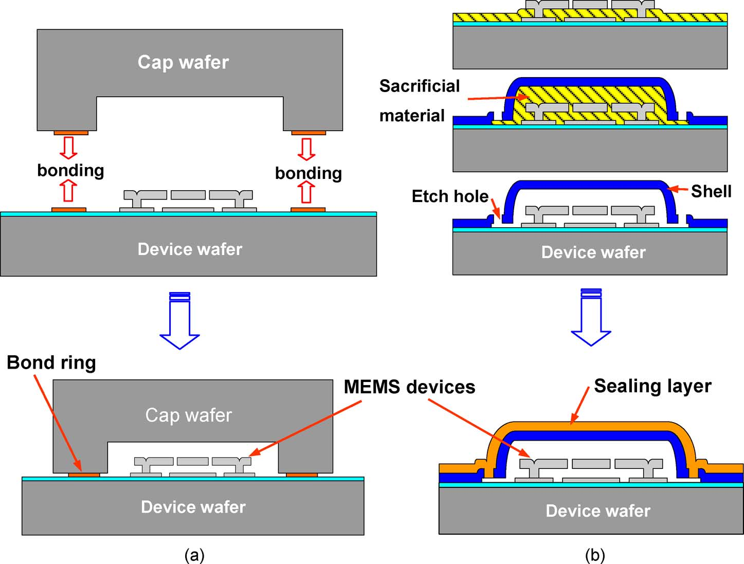
In general, the on-wafer encapsulation approaches fall into two categories: hybrid wafer bonding and monolithic thin-film encapsulation. In a hybrid approach (shown in the left column in Fig. 1), a separate substrate is bonded to the MEMS wafer to cap the MEMS components using a wide variety of bonding techniques, either in a form of direct surface bonding or using an intermediate layer . While wafer bonding has been proven and is being widely used in industry, monolithic thin-film encapsulation has been considered to be potentially more cost effective. In the monolithic approach, the process is carried out on the same wafer where the MEMS devices are fabricated by adding extra thin-film processing steps. Illustrated in the right column in Fig. 1, an additional sacrificial layer is deposited on top of an unreleased device and then covered by a thin-film encapsulation layer. After the sacrificial layer is removed through the etch holes in the encapsulation layer, the etch holes are sealed by thin films deposited on top of the encapsulation layer in an appropriate pressure condition. Compared with hybrid waferbonding, monolithic thin-film encapsulation has several advantages.

Fig1
Despite the anticipated advantages over the hybrid approach using wafer-bonding, the existing monolithic thin-film encapsulation methods suffer from a few drawbacks. Limited by the lithography and etching techniques, the etch holes patterned in the encapsulation shell have a typical size of a few micrometers. Opening vertical etch holes in the encapsulation layer above the device area is not preferable, because a significant amount of sealing material can easily diffuse through the etch holes and deposit on the device surfaces inside the cavity, changing the device characteristics. While this issue can be alleviated by utilizing laterally directed etch channels, it takes a long time to remove the sacrificial layer from the cavity, potentially degrading the mechanical properties of the structure material. Improperly designed lateral etch channels can also lead to excessive gas evacuation time during the sealing process.
A critical question in developing the proposed encapsulation technique is whether a free-standing porous polysilicon shell can be fabricated. Traditionally, nonsuspending layers of porous polysilicon were formed on top of conductive silicon, which provides a current path from the backside for electrochemical etching. For the unusual case of a nonconductive surface, Anderson et al. [22] have reported that polysilicon sandwiched between two nitride layers can be turned porous laterally by electrochemical etching. However, the porous polysilicon layer was sacrificed by electropolishing to form a nitride channel, rather than being released as a free-standing porous structure. It was not clear whether the polysilicon deposited on top of an insulator such as silicon dioxide and silicon nitride—a typical confifiguration in the polysilicon surface micromachining—can be turned porous through the entire thickness by electrochemical etching. If this is feasible and residual stress is controlled, a free-standing porous polysilicon membrane can be subsequently obtained by sacrificially removing the insulator material underneath through the pores.