Approaches to monolithic wafer-level threedimensional integrated circuits (3D ICs) generally involve bonding of processed wafers. Various bonding issues are described in this invited paper, focusing on the more stringent technology of back-end, monolithic, wafer-level 3D hyper-integration, aimed at forming highperformance, multifunctional nanosystems at the sub-100 nm technology node. The specific 3D technology approach considered in this paper consists of wafer bonding with dielectric adhesives, a three-step thinning process of grinding, polishing and selective etching, and an inter-wafer interconnect process using copper damascene patterning. The use of a dielectric bonding adhesive that provides robust wafer bonding and eases pre-bonding wafer planarization requirements is a key to process compatibility with standard IC and packaging processes. The desirable properties of dielectric bonding adhesives, bond strength and issues related to bonded functional IC layers with multilevel interconnects are discussed.
Experimental results show that benzocyclobutene (BCB) as a dielectric adhesive for wafer bonding has many advantages, including 1) the ability to accommodate wafer-level non-planarity (e.g., surface topography, wafer bow) and particulates at the bonding interfaces; 2) high bond strength; 3) relative low temperature bonding process as well as high temperature stability after bonding; 4) no degradation of the mechanical and electrical properties of state-of-the-art 130nm technology CMOS SOI test structures with fourlevel copper / low-k interconnects.
Future needs of dielectric bonding adhesives and thermal mechanical impacts of wafer bonding for 3D IC applications are also projected.

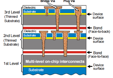
Fig1
Figure 1. Schematic of a monolithic 3D hyper-integration concept using adhesive wafer bonding and copper damascene inter-wafer interconnects, showing bonding interface, vertical inter-chip vias (plug- and bridge-type), and "face-to-face" and "face-to-back" bonding.
Figure 2. Semi-transparent image of two-level Cu/oxide interconnect structures bonded using BCB to a glass wafer, where the silicon substrate of the Cu/oxide interconnect structures is completely removed. The wafers with the Cu/oxide interconnect structures are provided by International SEMATECH. Though the surface profile (right) shows a step height of ~900 nm across the Al pads, void-free bonding using BCB is obtained and maintained after wafer thinning.