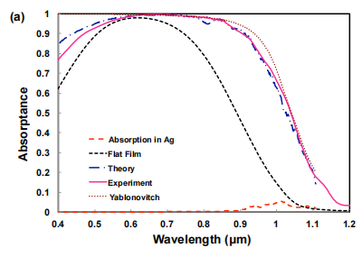
Thin-film c-Si solar cells with light-trapping structures can enhance light absorption within the semiconductor absorber layer and reduce material usage. Here we demonstrate that an inverted nano-pyramid light-trapping scheme for c-Si thin films, fabricated at wafer-scale via a low-cost wet etching process, significantly enhances absorption within the c-Si layer. A broadband enhancement in absorptance that approaches the Yablonovitch limit1 is achieved with minimal angle dependence. We also show that c-Si films less than 10μm in thickness can achieve absorptance values comparable to that of planar c-Si wafers thicker than 300μm that amounts to an over 30-fold reduction in material usage. Furthermore the surface area increases by a factor of only 1.7, which limits surface recombination losses in comparison with other nanostructured light-trapping schemes. These structures will not only significantly curtail both the material and processing cost of solar cells, but also achieve the high efficiency required to enable viable c-Si thin-film solar cells in the future.
Bulk c-Si solar cells dominate the photovoltaic (PV) market. Typically, c-Si wafers 180-300μm thick are used to ensure adequate absorption of sunlight, and this material accounts for about half of the total module cost.2, 3 In bulk crystalline Si solar cells, light-trapping is typically provided by randomly textured surfaces. 4 The characteristic size of these textures is typically 3-10µm, which is much larger than the wavelength of sunlight and not applicable for thin films. Thus various nanophotonic structures have been studied in recent years, including nanowires, nanoholes, nanocones, plasmonic particles, and photonic crystal surface structures.5-14 The efficiency of Si nanowire and nanohole-based solar cells6, 7, 15- 17 has been limited to ~10%, a value far smaller than the ~25% efficiency for state-of-the-art thick c-Si solar cells.18 One major reason for the low efficiency in solar cells with nanowires and nanoholes is the high surface recombination rates due to the large surface area, which is usually more than an order of magnitude larger than flat cells.19 It was recently reported that flat 10-20μm thick c-Si based solar cells can have conversion efficiencies up to 15%.20, 21 Our previous investigation into nano-pyramid structures has shown great promise to enhance light absorption in thin c-Si based solar cells while minimizing the surface area increase, but this was limited to simulation. In this paper, we experimentally show that c-Si thin-films with thicknesses less than 10µm can absorb as well as 300µm-thick flat c-Si substrates when they are decorated with inverted nano-pyramid structures.
We fabricated inverted nano-pyramids using standard scalable microfabrication techniques based on interference lithography (IL)25 and wet Si etching26. Figure 1(a) shows an optical image of the typical sample. The exposed area is limited by the exposure area of the IL tool to approximately 25mm × 25mm. It should be noted that IL can be applied to standard 156mm x 156mm wafers.27 Typical scanning electron microscope (SEM) images of the resulting structures are illustrated in Figs. 1(b) and (c). Figure 1(b) illustrates the top-view of inverted nano-pyramids with a periodicity of 700nm and a mean separation of 100nm between the pyramids produced after etching in a potassium hydroxide (KOH) solution. Figure 1(c) illustrates the cross sectional SEM of the resulting structure with the insets clearly showing the interfaces of the SiNx, Si, SiO2 and Ag layers. The sample illustrated here employed a 90nm thick SiNx, 10μm thick Si, 1μm thick SiO2, and 200nm thick Ag as antireflection coating, active absorbing medium, surface passivation and back-reflector, respectively. Because of the anisotropic etching of c-Si in the KOH solution, inverted nano-pyramids are formed at an angle of 54.7 degrees to the wafer surface, which is responsible for the factor of 1.7 increase in surface area.

Fig1
Inverted Nano-Pyramid fabrication. The fabrication process flow is as follows; First, a commercial silicon-on-insulator (SOI) wafer was acquired with the desired Si and SiO2 thicknesses. Then an array of holes was patterned in negative photoresist on the surface of the Si thin film using interference lithography (IL). Subsequent wet etching in an aqueous potassium hydroxide (KOH) solution was used to produce the inverted pyramids on the surface of the Si thin film and etch the backside of the Si handle wafer. KOH wet chemistry was chosen because it etches c-Si anisotropically yielding a self-aligned pyramid structure. Finally a SiNx anti-reflection coating was deposited on top of the inverted pyramids with plasma enhanced vapor deposition (PECVD) and a silver layer was deposited by evaporation on the backside of the SiO2 to simulate the Ag back contact of the photovoltaic module.