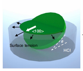
Epitaxial lift-off process enables the separation of III–V device layers from gallium arsenide substrates and has been extensively explored to avoid the high cost of III–V devices by reusing the substrates. Conventional epitaxial lift-off processes require several post-processing steps to restore the substrate to an epi-ready condition. Here we present an epitaxial liftoff scheme that minimizes the amount of post-etching residues and keeps the surface smooth, leading to direct reuse of the gallium arsenide substrate. The successful direct substrate reuse is confirmed by the performance comparison of solar cells grown on the original and the reused substrates. Following the features of our epitaxial lift-off process, a high-throughput technique called surface tension-assisted epitaxial lift-off was developed. In addition to showing full wafer gallium arsenide thin film transfer onto both rigid and flexible substrates, we also demonstrate devices, including light-emitting diode and metal-oxidesemiconductor capacitor, first built on thin active layers and then transferred to secondary substrates.
Gallium arsenide (GaAs), with its high electron mobility and direct bandgap, has been employed in high performance RF electronics and optoelectronics for decades1–4. On the basis of thermodynamics calculation, its bandgap lies at the energy for the theoretical maximum efficiency of single junction (SJ) solar cells and makes it an ideal material for high efficiency solar cells5. However, the high cost of GaAs substrates hinders them from being widely adopted in certain applications, in particular for solar cell because of a need for large amounts of the material. A typical thickness of a GaAs substrate is around a few hundred micrometres, and only a few micrometres or nanometres thickness is required to fully absorb the solar energy or serve as the active layer for device operation. Therefore, the material cost can be potentially reduced if thin device layers can be separated from the substrate while keeping the substrate intact and ready for another epitaxial growth.
In 1978, Konagai et al.6 proposed a method which is known today as epitaxial lift-off (ELO) to separate a device layer from a GaAs substrate by using hydroflfluoric acid (HF) to selectively etch a AlGaAs (aluminium compound) sacrificial layer inserted between the device film and the substrate (Fig. 1(a)). Subsequently, this same method has been applied by many researchers to successfully peel GaAs thin films from the parent substrates and transfer them onto desirable substrates for various applications7,8. The major drawback of this method arises from the high surface roughness of the parent substrate as well as reaction residues left on the substrate after the ELO process, and post-process steps, for example, chemicalmechanical-polish or chemical etching, typically required to reclaim the substrate9. In addition, HF is a lethal and highly corrosive acid requiring special handling and extra protection. Compared with typical short processing times with HF in silicon industry, the conventional ELO process takes hours to complete, which potentially increases the exposure risk for operators and the operating cost. Hence, developing a new ELO process with different chemistry that enables the direct reuse of the substrate is very desirable to lower the overall cost. Although HCl-based etchant was proposed and used by several researchers to selectively etch AlGaAs10,11 or other sacrificial layers12–14, the possibility of reusing the substrate directly with these methods has not been explored. In this paper, we demonstrate a new ELO process where aluminium-arsenide based sacrificial layer and HF-based etchant are replaced with phosphide-based materials and HCl. This new approach minimizes the amount of postetching residues and provides the surface passivation that keeps the surface smooth during ELO process, leading to direct reuse of GaAs substrate.

Fig1
Finally, one major throughput bottleneck in conventional ELO processes is the slow lateral etch rate of the sacrificial layer. Generally speaking, the lateral etch rate of the sacrificial layer is determined by two consecutive processes: the diffusion of the etchant from the solution to the etching front and the reaction of etchant with the sacrificial layer. The etch rate is initially limited by the chemical reaction until the diffusion distance of the etchant causes the etch rate to be limited by the diffusion rate. Performing the ELO process in the chemical reaction rate limited regime is preferred as it can maximize the overall etch rate. In order to do so, several methods with sophisticated setups, for example, weight-assisted ELO30 and etching assisted by roller15,31, were developed to accelerate the ELO process. However, these are only single-wafer solutions with consequent low throughput.
In conclusion, the direct reuse of GaAs substrates has been demonstrated by a newly developed ELO process. Residue-free and atomically flat post-ELO surfaces, resulting from the use of phosphide base sacrificial layers and HCl-based etchants, results in high quality regrown GaAs thin films and enables the regrowth of solar cell structures without observable performance degradation. Furthermore, STA-ELO, a high-throughput lift-off technique, is developed and employed to transfer GaAs thin films onto both rigid and flexible substrates. This technique opens up a suite of potential applications using III–V materials.