Unfortunately, the temperature window of perovskite oxides is rather narrow making the layer transfer a relatively difficult process . The present paper shows our latest achievements concerning layer splitting of oxide materials including the optimization of the implantation parameters as well as the annealing conditions for layer splitting. It also shows the transfer of small area single crystalline oxide layers with sub-micron thickness.
The as-implanted samples were annealed in air at a temperature ranging from 250◦C up to 700◦C. Nomarski optical microscopy, atomic force microscopy (AFM) and scanning electron microscopy (SEM) were used to investigate blister formation and exfoliation. Formation of platelet-like defects and their evolution after annealing were analyzed by cross section transmission electron microscopy (XTEM) at 200 kV. SEM and TEM were used also for investigation of transferred layers.
During implantation a high density of extended defects such as platelets, bubbles and micro-cracks are created. These defects are nucleation centers for the agglomeration of diffusing He or H during annealing. Both, blistering and layer splitting are connected with the evolution of micro-cracks filled with He and/or H. For as-implanted samples that are not bonded to another substrate surface blistering usually occurs during annealing. Layer splitting is observed if the implanted surface is stiffened by bonding the implanted wafer to a handling wafer.
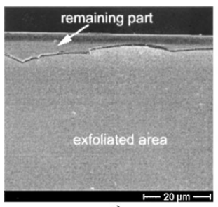
In order to find the optimum implantation conditions all samples were investigated directly after implantation and after annealing. It was observed that if the implanted temperature was above an optimum value blistering/exfoliation occurs directly during implantation. If the temperature during implantation is too low no blistering/exfoliation was obtained even after high temperature annealing (up to 700◦C). The optimum implantation conditions (presented in Table I) were determined by the lack of blisters in as-implanted substrates and their appearance after thermal treatment. As it can be seen in Table I STO and LNO require RT- implantation, while for PLZT and LAO higher implantation temperatures are needed (200◦C and 200–300◦C, respectively).

Fig1
Single crystalline substrates, implanted at optimum conditions (see Table I), were used for layer splitting. The first attempt to direct bonding failed due to a relatively high micro-roughness (e.g., the RMS roughness of the implanted STO and host STO substrate surfaces was about 1 nm). Therefore, different bonding procedures via various intermediate layers such as spin-on glass (SOG), Au, polymeric layer etc., were used to transfer oxide layers onto different substrates. Successful layer transfers of single-crystalline STO and LAO have been achieved by annealing of the bonded pairs at 300◦C (see Fig. 4). Nevertheless, due to non-homogeneity of the bonding interface and thermal mismatch, the transferred layers shattered into pieces of several hundred microns across. TEM investigations showed that the transferred STO layer is about 500 nm thick (Fig. 5), which agrees with the value calculated from TRIM (transport-of-ion-in-mater) simulation. The surface after splitting has a relatively high micro-roughness due to crack formation within the sacrifificial layer during post-implantation thermal treatment. The good crystal structures of the transferred layers remain after ion implantation, bonding and splitting, which was confirmed by diffraction pattern (Fig. 5, inset).