Heterogeneous integration of III-V semiconductor materials on a silicon-on-insulator (SOI) platform has recently emerged as one of the most promising methods for the fabrication of active photonic devices in silicon photonics. For this integration, it is essential to have a reliable and robust bonding procedure, which also provides a uniform and ultra-thin bonding layer for an effective optical coupling between III-V active layers and SOI waveguides. A new process for bonding of III-V dies to processed siliconon-insulator waveguide circuits using divinylsiloxane-bis-benzocyclobutene (DVS-BCB) was developed using a commercial wafer bonder. This “cold bonding” method significantly simplifies the bonding preparation for machine-based bonding both for die and wafer-scale bonding. High-quality bonding, with ultra-thin bonding layers (<50 nm) is demonstrated, which is suitable for the fabrication of heterogeneously integrated photonic devices, specifically hybrid III-V/Si lasers.
SOI is an emerging platform for photonic integrated circuits; it offers the potential of realizing low-cost and compact optical circuits. Moreover, standard complementary metal oxide semiconductor (CMOS) processing infrastructure can be used to process these optical components. This allows high-yield fabrication and a reduction of the component cost through economies of scale. However, the fabrication of efficient light sources in silicon photonics is challenging due to silicon’s indirect bandgap. Because of this indirect bandgap, the probability for an excited electron-hole pair to recombine and emit a photon is strongly reduced as a result of the much higher non-radiative recombination rate. Advances are being made to achieve light emission from silicon, either by modifying the silicon on a nanoscale or by exploiting its nonlinear optical properties. However, those devices are not good enough for use in high-performance sensing and communication systems. In order to create photonic integrated circuits comprising both opto-electronic and passive optical components, the heterogeneous integration of passive silicon-on-insulator waveguide circuits and active InP/InGaAsP components has been proposed, for applications in the telecommunication wavelength range.
While there are various methods to transfer an InP/InGaAsP epitaxial layer structure onto an SOI waveguide wafer (molecular bonding, adhesive bonding, anodic bonding, metallic bonding), adhesive bonding offers some significant advantages over the other bonding methods. The relaxed requirements on surface cleanliness, contamination and surface roughness combined with the planarizing action of the adhesive spin coating process, offer a significant reduction in surface preparation. Moreover, the integration process is a lowtemperature process, reducing the stress in the bonded stack due to the difference in thermal expansion coefficients between silicon and III-V semiconductor.
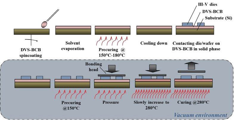
In this paper, we describe a new adhesive wafer bonding process scheme that involves partial curing of the DVS-BCB prior to bonding and attaching the III-V substrate at room temperature prior to curing in a vacuum atmosphere. This “cold bonding” method significantly simplifies the bonding preparation for machine-based bonding, both for die and wafer-scale bonding. This approach shows high yield for ultra-thin bonding thicknesses below 50 nm, as well as a good uniformity of the DVS-BCB layer thickness after wafer bonding over the full wafer area. This process was applied to achieve ultra-thin DVS-BCB bonding layers for the fabrication of several photonic devices, such as III-V/SOI lasers.

Fig1
Several bonding experiments were performed to evaluate the bonding quality and the DVSBCB thickness uniformity after wafer bonding. The experimental results are discussed in the following sections. Wafer-to-wafer, die-to-wafer and multiple die-to-wafer bonding are reported.
The bonding quality was first assessed by bonding 2 inch InP wafers to 4 inch Pyrex glass wafers (with a thermal expansion coefficient similar to that of silicon). In this way, the bonding interface can be inspected through the Pyrex substrate using a standard microscope with a polarization filter. The InP wafer was etched away after bonding using a selective wet etching solution (HCl) to measure the thickness and uniformity of the DVS-BCB bonding layer. The results of 5 wafer bonding experiments are summarized in Table 1, showing a good uniformity over the wafer (the bonding layer thickness was measured in 18 points all over the wafer area using a profilometer) and a good reproducibility of the nominal bonding layer thickness, even when there is a variation in applied pressure. A DVS-BCB:mesitylene dilution of 1:8 (v/v) was used in the experiment; spin coated at 3000 rpm, this results in a 35 nm DVSBCB bonding layer thickness. Even with such thin bonding layers, the bonded area is above 99%. The non-bonded parts are due to the presence of particles at the bonding interface. This is related to the fact that bulk InP wafers were used without a sacrificial InP/InGaAs layer pair to remove particle contamination from the surface.
上一篇: 离子注入和直接晶圆键合的单晶铁电薄膜
下一篇: 转移化学气相沉积在石墨烯的残留的金属污染