Carrier collection in silicon heterojunction (SHJ) solar cells is usually achieved by doped amorphous silicon layers of a few nanometers, deposited at opposite sides of the crystalline silicon wafer. These layers are often defect-rich, resulting in modest doping efficiencies, parasitic optical absorption when applied at the front of solar cells, and high contact resistivities with the adjacent transparent electrodes. Their substitution by equally thin doped nanocrystalline silicon layers has often been argued to resolve these drawbacks. However, low-temperature deposition of highly crystalline doped layers of such thickness on amorphous surfaces demands sophisticated deposition engineering. In this paper, we review and discuss different strategies to facilitate the nucleation of nanocrystalline silicon layers and assess their compatibility with SHJ solar cell fabrication. We also implement the obtained layers into devices, yielding solar cells with fill factor values of over 79% and efficiencies of over 21.1%, clearly underlining the promise this material holds for SHJ solar cell applications.
Various groups have reported approaches to minimize incubation layers, and excellent results have been obtained by optimizing the deposition parameters (temperature, pressure, power, silane dilution, frequency) . Pretreatments of the surface or deposition of buffer layers have also been explored, to induce fast nucleation. Furthermore, specifific deposition procedures, like the sequential deposition/etching (layer-by-layer) method, have been applied successfully.
In this paper, we focus specifically on the integration of borondoped [μc-Si:H(p)] and phosphorous-doped [μc-Si:H(n)] layers into SHJ solar cells, while satisfying the requirements mentioned above. This paper outlines strategies to obtain ultrathin nanocrystalline silicon films applicable for SHJ solar cell fabrication but mentions also the unsuccessful approaches that result in poor device performance. Due to the amorphizing impact of boron on layer growth, we specifically focus on p-type μc-Si:H layers. We also report cell results obtained with both p- and n-doped μc-Si:H layers deposited using different plasma regimes and with different device architectures.
Selected layers were deposited on a-Si:H-coated, double-side polished wafers with (1 1 1) crystallographic orientation. Polished wafers were used to facilitate the subsequent analysis of the transmission electron microscopy (TEM) micrographs. These samples were processed into cross-sectional specimen by focused ion beam milling for high-resolution TEM investigations. A fifinal thinning step was performed with low energy Ar ions (0.5 eV) using a Fischione NanoMill system. Structural investigations were performed using an FEI Titan microscope equipped with a spherical aberration corrector at the image plane with a beam energy of 300 kV.

Fig1
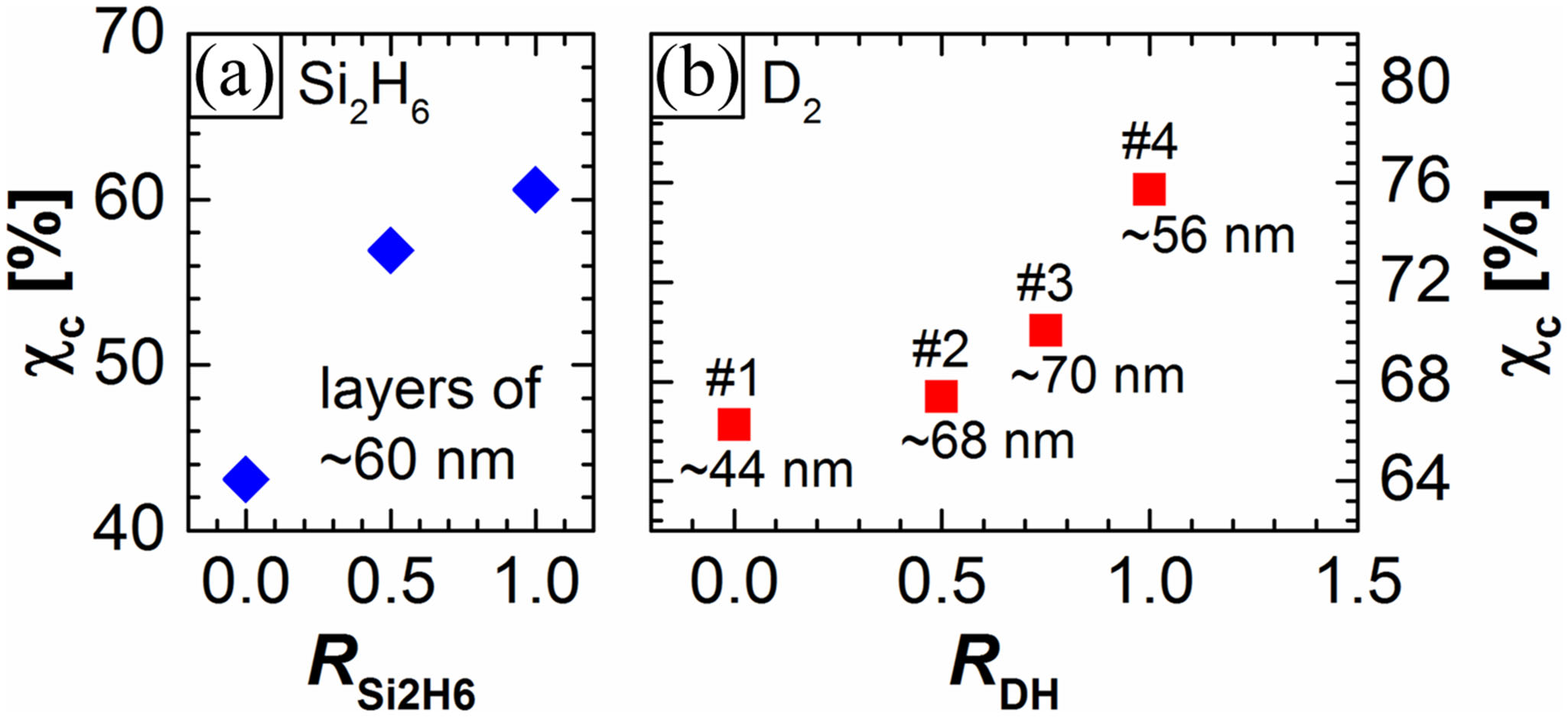
While the deposition of an a-SiOx :H buffer can help on layer level, this method is prone to lead to inferior cell performance, if applied to the hole-collecting side, which is linked to the insertion of oxide-related transport barriers into the contact stack. All the non-standard gases applied here (SiF4 , Si2H6 , and D2 ) were shown to potentially increase χc of the layers and are applicable to SHJ devices. Lowering the temperature does not represent a harmful measure on device level and was shown to increase χc . Higher deposition frequencies were shown to enable highly crystalline nanometer-scale layers, which, however, may exhibit a lower material quality. Despite this latter possible drawback, as shown in the next section, devices with decent open-circuit voltage (Voc ) values were fabricated also at very high deposition frequencies.
上一篇: 硅太阳能电池的红外线研究
下一篇: 硅晶片的激光清洗:机制和效率