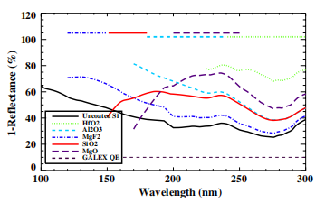
We report on the development of coatings for a charged-coupled device (CCD) detector optimized for use in a fixed dispersion UV spectrograph. Because of the rapidly changing index of refraction of Si, single layer broadband antireflection (AR) coatings are not suitable to increase quantum efficiency at all wavelengths of interest. Instead, we describe a creative solution that provides excellent performance over UV wavelengths. We describe progress in the development of a coated CCD detector with theoretical quantum efficiencies (QEs) of greater than 60% at wavelengths from 120 to 300 nm. This high efficiency may be reached by coating a backside-illuminated, thinned, delta-doped CCD with a series of thin film AR coatings. The materials tested include MgF2 (optimized for highest performance from 120–150 nm), SiO2 (150–180 nm), Al2O3 (180–240 nm), MgO (200–250 nm), and HfO2 (240–300 nm). A variety of deposition techniques were tested and a selection of coatings that minimized reflectance on a Si test wafer were applied to functional devices. We also discuss future uses and improvements, including graded and multilayer coatings.
Charged-coupled devices (CCDs) were first invented at Bell Labs in 1969, and have since revolutionized imaging. The CCD’s ability to quickly and efficiently digitize data, its relatively low noise capabilities, and a sensitivity of 100 times that of film meant that they quickly became indispensable to modern astronomy . For UV astronomy, CCDs have not historically been a success. While film is sensitive at nearly all wavelengths of light, unmodified CCDs present a number of deficiencies. The front circuitry of a CCD is absorptive at UV wavelengths. For high efficiency, CCDs are back illuminated; however, the Si substrate is, in turn, highly reflective. More crucially, UV photons have a very short absorption depth in Si. The resulting electron–hole pairs find traps at the surface and never reach the gates for eventual readout. These characteristics have created problems in developing efficient CCD-based UV detectors. One notable work-around to these issues was used for the Wide Field Planetary Camera 2 (WFPC2) on the Hubble Space Telescope (HST) . WFPC2 used thick, front-illuminated CCDs but coated them in a layer of the UV phosphor Lumogen, which provided a UV response of 10%–15% from 200 to 400 nm by downconverting the UV photons to 510–580 nm photons. The current camera on HST, WFC3, also utilizes a CCD (thinned and backside illuminated with a charged backside) and antireflection (AR) coating for the near-UV (NUV), but has a few percent quantum efficiency (QE) hysteresis . Other types of UV detectors have been developed and are in use on current missions, including microchannel plates (MCPs) (such as JUNO , FUSE , GALEX , ALICE , and FIREBall , to name a few). While their photon-counting capabilities make them useful and they have no red leak problems, MCPs still suffer from low QE [25% in the far-UV (FUV, 1344– 1786 Å) down to 8% in the NUV (1771–2831 Å) for the GALEX MCPs] and are challenging to produce and utilize. In this work, we examine an improved CCD that is able to overcome the difficulties described above.
We have selected MgF2, MgO, HfO2, Al2O3, and SiO2 to test as suitable AR coatings. The materials chosen reflect the unique requirements of a UV AR coating, including a favorable index of refraction and low absorption in the desired waveband. One must be able to deposit the film in a uniform way, while not causing damage to the CCD itself. This eliminates electron beam evaporation (a common choice for dielectric coatings) as a potential technique because it causes x-ray damage to the CCDs. We have tested sputtering, atomic layer deposition (ALD), and thermal evaporation techniques for consistency and measured the reflectance of films on a substrate of uncoated Si. This is a low-cost, faster alternative to testing on functional devices. The downside is that testing is limited to reflectance off this surface, which necessarily omits any absorption losses. We then compare our measurements to the theoretical models. A further discussion of deposition techniques and their effect on film quality will be presented in a forthcoming paper.

Fig1
Thicknesses that provided close to peak transmission while also maintaining a wide range above 50% were selected. The reflectance that corresponded to this thickness was then used as a target during testing. We sought to make a range of film thickness that were centered around this target. Typically, we tested several films that varied in thickness between 5 and 10 nm above and below the target. There are several published indices of refraction for the Si substrate, which contributes to some uncertainty in the predicted reflectance. The indices of refraction for all materials were taken from Palik, except for HfO2, which came from Zukic et al.. An alternative index of refraction for Si was also consulted, taken from Philipp and Taft . The Philipp values differed at the shortest wavelengths (below 150 nm) and predicted a lower reflectance than the Palik values.
Further tests were done to ensure reliability. Two to three films were made for each material with the same deposition process as the best-fit film. Two things were tested here: the repeatability of the deposition procedure and consistency of performance from sample to sample. Deposition of all have proven to be quite repeatable (thicknesses vary by 1 nm from target) and are especially repeatable for ALD depositions. The values for reflectance are also consistent across samples of the same material.