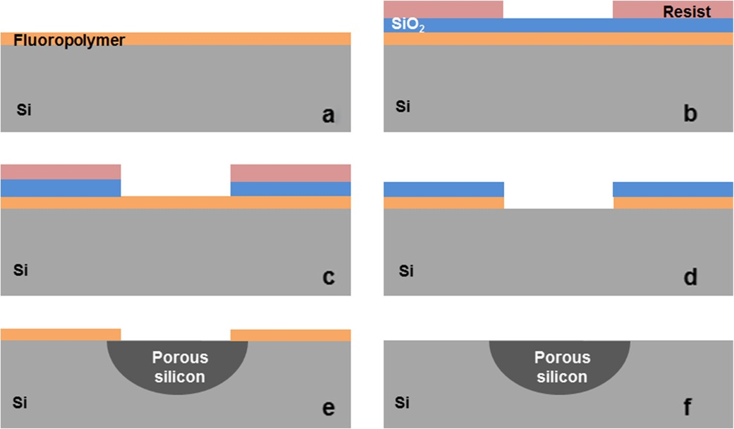
The study of an innovative fluoropolymer masking layer for silicon anodization is proposed. Due to its high chemical resistance to hydrofluoric acid even under anodic bias, this thin film deposited by plasma has allowed the formation of deep porous silicon regions patterned on the silicon wafer. Unlike most of other masks, fluoropolymer removal after electrochemical etching is rapid and does not alter the porous layer. Local porous regions were thus fabricated both in p+ -type and low-doped n-type silicon substrates.
Silicon electrochemical etching is known as a low-cost technique to rapidly and easily produce large areas of porous silicon (PoSi). The large range of possible morphologies of PoSi makes it an attractive material for numerous applications. Micro- and mesopores (i.e., with pore diameter< 2 nm and 2 to 50 nm, respectively) are intensively studied in photoluminescence, microelectromechanical systems (MEMS), or RF device domains, whereas macropores may be employed in through-silicon via (TSV), photonics, or membrane applications. Despite the wide range of applications and its low production cost, silicon anodization suffers from several issues that limit its industrialization. The localization of porous regions on the silicon wafer is the most restrictive one, especially for microelectronic applications.
The reason of localization issues is directly linked to the fabrication process. The PoSi is produced in hydrofluoric acid (HF)-based solutions, often at high acid concentration. This acid is highly corrosive; thus, only few materials are chemically resistant in this solution for long-duration anodizations since some specific applications require the formation of deep local PoSi regions. Moreover, for some materials, the application of an anodic bias during the PoSi formation may affect their chemical stability.
For most of the above-mentioned applications, the mask must be removed after local anodization. Moreover, the mask removal must not deteriorate the underlying porous layer. Micro- and mesoporous layers are very sensitive to their chemical environment and to the temperature because of their high developed surface. A mask removal technique that also etches or oxidizes the PoSi is thus forbidden. Regarding the macropores, their thick sidewalls and lower developed surface ensure a relative chemical resistance compared to micro/mesoporous layers.

Fig1
Figure 2 exhibits the quasi-isotropic etching behavior in this material since PoSi is fabricated under the mask. For a given anodic current density, the under-mask etching seems to be proportional to the PoSi thickness (Figure 3). Ratios from 0.5 to 0.7 were obtained between the under-mask etching length and the PoSi thickness.
Different pattern densities were also analyzed in the same substrate: the highest is the pore density; the worst are the edges to ensure a stable pore growth in the middle of the opened area. The higher current density (respectively, bias) that must be provided to ensure a stable pore growth is assumed to be responsible for this behavior. To increase the pattern density, the objective is to decrease the substrate resistivity to reduce the stable growth current density .
下一篇: 用于硅探测器设计的紫外线抗反射涂层