Thin 50-µm silicon wafers are used to improve heat dissipation of chips with high power densities. However, mechanical dicing methods cause chipping at the edges of the separated dies that reduce the mechanical stability. Thermal load changes may then lead to sudden chip failure. Recent investigations showed that the mechanical stability of the cut chips could be increased using ultrashort-pulsed lasers, but only at the laser entrance (front) side and not at the exit (back) side. The goal of this study was to find strategies to improve both front- and backside breaking strength of chips that were cut out of an 8″ wafer with power metallization using an ultrafast laser. In a first experiment, chips were cut by scanning the laser beam in single lines across the wafer using varying fluencies and scan speeds. Three-point bending tests of the cut chips were performed to measure front and backside breaking strengths. The results showed that the breaking strength of both sides increased with decreasing accumulated fluence per scan. Maximum breaking strengths of about 1100 MPa were achieved at the front side, but only below 600 MPa were measured for the backside. A second experiment was carried out to optimize the backside breaking strength. Here, parallel line scans to increase the distance between separated dies and step cuts to minimize the effect of decreasing fluence during scribing were performed. Bending tests revealed that breaking strengths of about 1100 MPa could be achieved also on the backside using the step cut. A reason for the superior performance could be found by calculating the fluence absorbed by the sidewalls. The calculations suggested that an optimal fluence level to minimize thermal side effects and periodic surface structures was achieved due to the step cut. Remarkably, the best breaking strengths values achieved in this study were even higher than the values obtained on state of the art ns-laser and mechanical dicing machines. This is the first study to the knowledge of the authors, which demonstrates that ultrafast-laser dicing improves the mechanical stability of thin silicon chips.
Miniaturization and performance enhancement of consumer electronic products drive the development of new emerging chip fabrication technologies. Thinned silicon wafers with thicknesses of about 50 µm enable higher packaging densities for three-dimensional (3D) silicon integration and reduce the heat resistance to improve heat dissipation for increasingly powerful chips. Moreover, thinning increases the mechanical flexibility of the wafers, which enables the utilization of thin silicon wafers for bendable and flexible devices . However, the reduction of the wafer thickness causes new problems for established dicing methods.
Mechanical dicing becomes more challenging because the diamond blades of the saw cannot resharpen themselves at the thin wafer edges in the range of 100 μm or less . Moreover, mechanical dicing causes chippings at the edges that reduce the mechanical stability of the chip. Thermal load changes may then lead to sudden chip failure. The fracture strength of a mechanically diced wafer with a thickness of 50 µm is about 666 MPa . Since laser dicing is a contact-free method, chippings at the edges can be avoided. Consequently, the challenges for laser dicing are to improve the mechanical stability of the cut chips and to achieve the cutting speed of a wafer saw, which is in the order of 100 mm/s.

Fig1
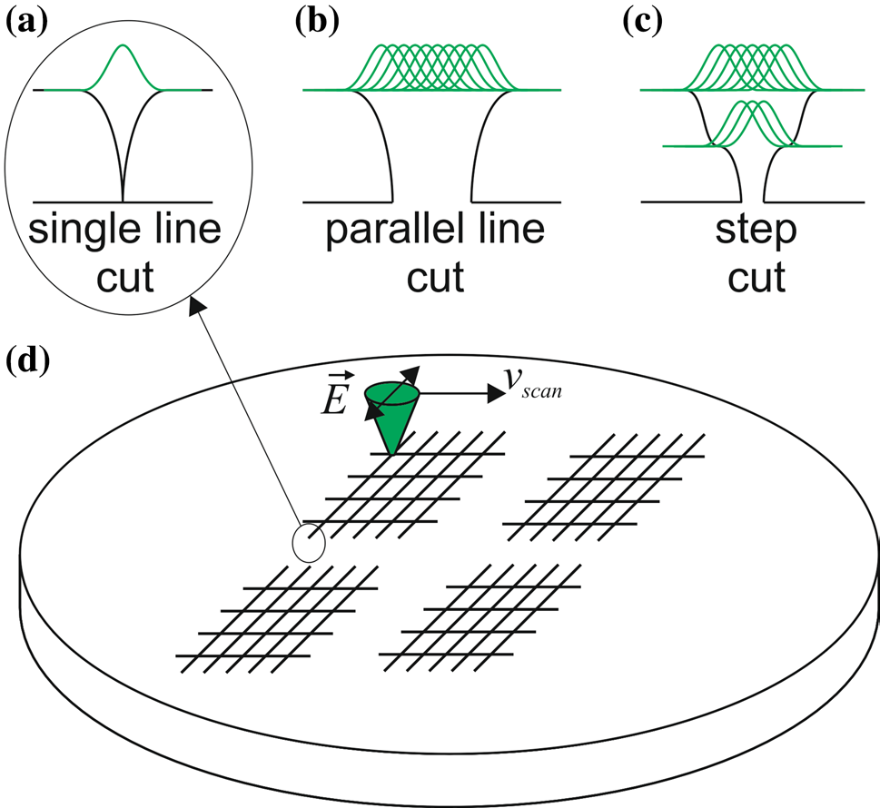
The chips for mechanical testing were prepared by dividing a wafer in four quadrants and cutting a matrix of 13×19 chips per quadrant and parameter set (see Fig. 1d). In this way, a safety distance of about 5 mm to the edges of the maximum scan field size was maintained to ensure homogeneous energy distribution in the processed area. The cut chips were picked always in the same order by starting from one of the corners and removing them line by line. In this way, chip location-dependent effects should have similar contribution to the statistic in the bending-test experiments. It should be mentioned here that influences of the chip location were not recognized in the bending test results. Due to the small chip size, special care had to be taken during picking and placing the chips. Picking was particularly difficult because the chips had to be separated from the dicing tape. If the polymer tape was not cut, the chips were lifted from the tape with a small knife. Special care was taken that the knife edge did not touch the sides being bended during mechanical testing. For this purpose, chips were only picked from every second line and the chips in between were sacrificed. In the case that the polymer tape stuck to the backside of the chip, it was peeled off carefully with the finger nail. The chips were then placed by hand in a bending test machine.
The parallel line cuts were performed using different combinations of pulse energies and numbers of scans. However, it was not possible to achieve breaking strengths higher than 600 MPa. These findings indicate that widening of the trench does not improve the backside breaking strength significantly.
下一篇: 超声波晶片测温中的薄膜效应