A lithographic approach to generate clean patterns of multiple types of nanoparticles on one 4-inch silicon wafer is demonstrated in this paper. Each type of nanoparticle is precisely directed to the desired location. The process is mainly based on conventional microelectronic techniques with extremely high reproducibility. This enables the possibility of industrial applications to fabricate devices made of nanocrystals. A thin film of polystyrene spheres, 150 nm in diameter, was first coated on the silicon wafer with layer-by-layer self-assembly, followed by a layer of aluminum deposited on the thin film. A layer of positive photoresist was spun on the surface of aluminum and then patterned by lithographic technique. The unprotected aluminum was removed by wet etching until the polystyrene thin film underneath was exposed to the air. Oxygen plasma was employed to etch the polystyrene thin film all the way to the silicon surface. Subsequently, a thin film of another type of nanoparticle, silica particle 78 nm in diameter, was adsorbed onto the surface with layer-by-layer self-assembly. Eventually, aluminum and photoresist were removed and each type of nanoparticle was located next to each other as the pattern was designed. A scanning electron microscope was used to produce the image of the pattern.
Nanoparticles have been the focus of many material researchers due to their unique properties in the microelectronics, optoelectronics, and chemical fields. A great deal of attention has been attracted to the various potential applications of nanoparticles to complex nanoelectronic devices, photonic crystals, and biochemical sensors. Among numerous nanoparticle deposition techniques, layer-by-layer (LbL) self-assembly, since its introduction by Decher et al.,8,9 has become, due to its simplicity and versatility, an increasingly popular technique, which enables adsorption of colloidal nanoparticles onto almost any material. The alternate immersion of substrate in oppositely charged solutions allows thin films of nanoparticles, enzymes, or protein in nanometer scale to be coated by electrostatic interaction.
However, before the LbL self-assembled nanoscale colloidal structure is applied to real devices, an approach must be developed to easily generate complex and distinct patterns on the multilayer films. Recently, some results have been reported for the creation of spatially resolved nanoparticle films. These works are mostly based on the microprinting technique in which a template is first fabricated by stamping two functional chemicals on the flat substrate, then directing nanoparticles onto adhesion-promoting regions while they are repelled by adhesion-resisting regions. This method is quite successful but is restrictive in application by the necessity of special microstamps and the deliberate selective deposition. They are all chemical methods in principle. Another challenge prior to device fabrication is to pattern two or more types of nanoparticles on one wafer. Hammond and T. Vossmeyer groups demonstrated their approaches to introduce two types of nanoparticles in the matrix by selective deposition technique.

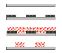
Fig1
In our early reports, two methods based on the combination of traditional lithography and LbL assembly were presented to pattern one type of nanoparticle film. One is referred to by authors as the “modified lift-off”, the other as the “metal-mask method”. The strategy completely differs from the microprinting technique, thus avoiding the difficult selective deposition. The patterns created by this strategy are illustrated in Figure 1. Since the standard 4-inch wafer process was adopted to pattern the LbL assembled nanoparticle films, dramatically high reproducibility is obtained on the whole wafer surface. In addition, each step of LbL self-assembly can be automatically controlled; therefore, this idea may find wide industrial application in the future. The schemes of both methods are illustrated in Figure 1.
During the lift-off, it is better to introduce ultrasonic treatment for 3 s when the wafer was soaked in developer solution. Within the nanoparticle film structure, polyion multilayers such as PDDA and PSS were sandwiched between the nanoparticle film and photoresist as a kind of “chemical glue”. The structure of the polyion is like a long thread which strongly links the polyion film as a whole. It is hard to break them up during the lift-off so that at some areas the nanoparticle and polyion multilayer cannot be removed when the photoresist is dissolved. On the contrary, they just come down and re-attach to the film underneath. The ultrasonic treatment is introduced to disconnect the linkage between polyion branches and to obtain a more distinct pattern with higher reproducibility.