Hydrogen and/or helium implantation-induced surface blistering and layer splitting in compound semiconductors such as InP, GaAs, GaN, AlN, and ZnO are discussed. The blistering phenomenon depends on many parameters such as the semiconductor material, ion fluence, ion energy, and implantation temperature. The optimum values of these parameters for compound semiconductors are presented. The blistering and splitting processes in silicon have been studied in detail, motivated by the fabrication of the widely used silicon-on-insulator wafers. Hence, a comparison of the blistering process in Si and compound semiconductors is also presented. This comparative study is technologically relevant since ion implantation-induced layer splitting combined with direct wafer bonding in principle allows the transfer of any type of semiconductor layer onto any foreign substrate of choice—the technique is known as the ion-cut or Smart-Cut method. For the aforementioned compound semiconductors, investigations regarding layer transfer using the ioncut method are still in their infancy. We report feasibility studies of layer transfer by the ion-cut method for some of the most important and widely used compound semiconductors. The importance of characteristic values for successful wafer bonding such as wafer bow and surface flatness as well as roughness are discussed, and difficulties in achieving some of these values are pointed out.
In this review, we discuss the phenomena of surface blistering and layer splitting in compound semiconductors such as GaAs, InP, GaN, AlN, and ZnO. Moreover, we report on feasibility studies of layer transfer by the ion-cut method for these semiconductors. The importance of characteristic properties of the wafers such as bow, flatness, and roughness for the wafer bonding process is discussed. In addition, the difficulties in obtaining some of these critical values are pointed out. The organization of this article is as follows: first a brief outline of blistering and splitting in semiconductors will be given, followed by different sections addressing each compound semiconductor individually. Finally, conclusions and the scope for future work will be presented.
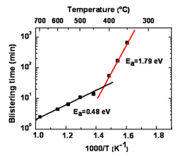
As in the case of GaAs, InP is also very sensitive to implantation temperature for observing controlled blistering/splitting. One reason behind the narrow temperature window could be the high diffusivity of hydrogen in these semiconductors, which may result in the loss of hydrogen from the damaged region during higher-temperature implantation. Since a minimum amount of hydrogen inside the damaged region is required to form the microcracks that subsequently result in surface blistering, its depletion from this region due to outdiffusion results in the absence of blistering/splitting. The microscopic details of this process in GaAs and InP need to be investigated further to make conclusive comments on the implantation temperature sensitivity of these semiconductors.

Fig1
The authors are thankful to the German Federal Ministry of Education and Technology (BMBF) for partial support in the framework of the CrysGaN project. Part of the work reported has been supported financially by the Max Planck Society (MPS), Germany, under the Indo-German cooperation scheme of the Max Planck India Partner Group and co-funded by the Department of Science and Technology (DST), India. Partial support via the research project nanoSTRESS jointly funded by the Max Planck Society and the Fraunhofer Society is also acknowledged.