With the introduction of 300 mm wafer and sub-100 nm technology processes, semiconductormanufacturers are gradually paying attention to efficient methods for process and equipment controlwhich is conventionally called advanced process control (APC) and advanced equipment control(AEC). As a potential strategy, an APC/AEC technique by selfexcited electron resonanceSpectroscopy (SEERS) was evaluated in a dynamic random access memory gate etch process, inlerms of chamber maintenance and process control. Small changes in the chamber conditions afteiwet cleaning, which could not be detected under conventional monitoring methods, were identifiedby analyzing the electron collision rate of plasma. This event justifies that plasma monitoring isinevitable in chamber maintenance, especially considering that process results gradually tend to beaffected by even small chamber changes in sub-100 nm technology process era. Also, the first wafereffect, one of the most serious process drifts in an etch process, could be clearly detected bycomparing average electron collision rates of plasma during each wafer process. In addition, astrong correlation between average electron collision rate and remaining oxide thickness enables usto control the gate etch process more tightly. Consequently, the APC/AEC technique by SEERS isexpected to be a potent strategy for plasma etch processes in semiconductor manufacturing.
Competition for manufacturing higher performance deices in a cost eflective way is accelerating the introductionof 300 mm wafer and sub-100 nm technology processes insemiconductor industries. The larger size of 300 mm wafermakes it possible for semiconductor manufacturers to fabri-cate some extra devices under the same process sequencesBesides, sub-100 nm technology processes can improve theperformance of devices as well as fabrication productivity.However, in order to take advantage of' these benefits, thereare some issues to be solved beforehand. That is, increasedsize of wafer might induce severe wafer-level uniformity issues. Adoption of sub-100 nm technology processes resultsin smaller process windows. Plasma etching processes.which are considered as key processes in semiconductormanufacturing, are also in these situations. To make mattersworse, various etch schemes are often required to breakthrough current technology limits. Consequently, there areincreasing demands for advanced process control (APC) andadvanced equipment control (AEC) techniques in the plasmaetching processes.
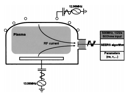
In this article, we introduced a potential APC techniquethrough real-time plasma monitoring. Self-excited electronresonance spectroscopy (SEERS), which gives physical in-formation on plasma without any disturbance on chamber13conditions.was adopted in order to achieve an APC tech-nique. First, we investigated the monitoring capability of SEERS in our plasma reactor, and then monitored gate etchprocesses for dynamic random access memory (DRAM)manufacturing by using SEERS. We also checked if there areany correlations between process results and monitoredSEERS data. Through these procedures, we will emphasizethe necessities of plasma monitoring for enhanced chambermaintenance and process fault detection.

Fig1
Ar plasmas under various activation conditions were firstmonitored in order to check monitoring capability of' SEERSin DPSm, and then the tungsten silicide etch processes forDRAM gate electrode were analyzed by using the electroncollision rate of the process plasma. The analyzed resultswere also compared to process results such as the remaininggate oxide thickness and the etched profile, measured with aspectroscopic ellipsometer and a scanning electron microscope, respectively.