A wide bandgap, an enhanced piezoelectric coefficient, and low dielectric permittivity are some of the outstanding properties that have made ScxAl1−xN a promising material in numerous MEMS and optoelectronics applications. One of the substantial challenges of fabricating ScxAl1−xN devices is its difficulty in etching, specifically with higher scandium concentration. In this work, we have developed an experimental approach with high temperature annealing followed by a wet etching process using tetramethyl ammonium hydroxide (TMAH), which maintains etching uniformity across various Sc compositions. The experimental results of etching approximately 730 nm of ScxAl1−xN (x = 0.125, 0.20, 0.40) thin films show that the etch rate decreases with increasing scandium content. Nevertheless, sidewall verticality of 85◦~90◦ (±0.2◦ ) was maintained for all Sc compositions. Based on these experimental outcomes, it is anticipated that this etching procedure will be advantageous in the fabrication of acoustic, photonic, and piezoelectric devices.
Like any other group III-V material, ScxAl1−xN can be etched by dry or wet etching techniques. One of the known dry etching approaches is ion beam etching, which can be physical or chemical and can result in smooth etched surfaces at a suitable etch rate. Table 1 summarizes experiments that dry etch ScxAl1−xN and reports sidewall verticality and etch rate. Luo et al. performed ICP etching with thick S1818 photoresist (PR) as an etch mask. They demonstrated how RF power might control the sample’s plasma etching energy, and how the energy of the Cl2/BCl3/N2 plasma enhances the sidewall angle of Sc0.06Al0.94N. James et al. demonstrated that the reactive ion beam etching (RIBE) process of ScxAl1−xN etching is superior to ion beam etching (IBE) in terms of etching rate, selectivity, and sidewall angle (73◦ ) (See Table 1). The ScxAl1−xN etching rate and selectivity degrade when the identical beam parameters (See Table 1) are used without the reactive gas . Wang et al. presented the design, fabrication, and characterization of Sc0.20Al0.80N thin films used for piezoelectric micromachined ultrasound transducers (PMUTs) by using RIE as an etching process (See Table 1). They claimed that the etched layer has good verticality and concluded that increasing the scandium concentration would enhance PMUT performance .
Hardy et al. attempted ICP etching using argon (Ar) rather than the more commonly used nitrogen and found that the etch selectivity is significantly higher for ScxAl1−xN relative to AlN and the surface roughness can be kept unchanged after etching process . Furthermore, Shao et al. successfully fabricated a lamb wave resonator with a quality factor of around 1000 with Sc0.22Al0.78N by achieving a 77◦ sidewall . They also concluded that Cl2 gas increases the anisotropy of the etching process since the dry etching process is mainly Cl2/BCl3 based. However, due to ScCl3’s poor volatility, performing dry etching of ScxAl1−xN can be an ineffective process . On the contrary, it takes more etching power and ion bombardment to get the etching rate back to a considerable level . Moreover, it was found that excessive etching into the bottom layer might be a concern for device fabrication, and a lower etching rate as well as high-power consumption are the fundamental causes of poor selectivity to various mask materials, which has accelerated the wet etching trials in the research community .

Fig1
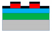
To pattern the SiO2 hard mask, a Ni metal film was used as the mask that was patterned using a lift-off process. After SiO2 deposition, lithography was conducted using an MLA 150 Advanced Maskless Aligner Heidelberg Instrument. During the process, AZ5214E photoresist (PR) is spin coated onto the sample at 5000 rpm, resulting in a thickness of 1.2~1.4 microns to prepare for a nickel lift-off process for SiO2 patterning. The sample(s) were pre-baked at 110 ◦C for 4 min, then exposed at 405 nm UV light at 135 mJ/cm2 , developed in AZMIF-300 for 45~50 s, and rinsed in diluted water for 25–30 s. Subsequently, using e-beam evaporation, a 100-nm thick nickel (Ni) film was deposited, which will eventually serve as a mask during the etching of SiO2 layer (See Figure 2).
During the Ni-metallization process, the base chamber pressure and evaporation pressure were maintained at 3.3 × 10⁻⁷ Torr, and 1.2 × 10⁻⁶ Torr, respectively. The deposition process was performed at 0.5 Å/s. After Ni deposition, the samples were immersed in an acetone solution for 15 min to remove the lift-off photoresist and expose the required regions for SiO2 etching. A post-clean was later used on all samples that consisted of an acetone, IPA, and DI water rinse.