Single-crystalline inorganic semiconductor nanomembranes (NMs), which have a thickness of less than a few hundred nanometers, have gained increasing interest since 2005 due to their remarkable use for a variety of applications. These free-standing NMs can be transferred to any arbitrary foreign substrates by using elastomeric stamps, which was first demonstrated by Meitl et al.Importantly, these NMs are compatible with the traditional semiconductor manufacture approach for fabricating various heterogeneously integrated and flexible electronic devices, including the seamless integration of semiconductor NMs with the low-cost, complementary-metal-oxidesemiconductor-compatible silicon (Si) substrates. Until now, several applications of transferrable monocrystalline NMs based on Si,germanium (Ge),gallium arsenide (GaAs)/aluminum gallium arsenide (AlGaAs),gallium nitride (GaN)/aluminum gallium nitride (AlGaN),[27–30] silicon carbide (SiC), gallium oxide (Ga2O3), etc. have been reported during the last few years. These transferrable narrow, wide, and ultrawide bandgap NMs have enabled a variety of device applications over the past nearly two decades.
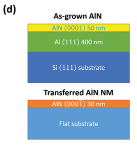
Initially, the AlN layer was grown using MBE and further, it was successfully transferred onto a flat sapphire (Figure S1, Supporting Information), a flat Si (Figures 2a,b and 3a), and a hexagon pillar-structured Si (Figure 1a–c) substrates. Figure 1a exhibits the optical image of the transferred AlN NMs on the pillar-structured Si substrate. The pillar-structured Si substrate was prepared via photolithography and reactive ion etching (RIE) and the height of the pillars is about 4 µm. The pillars can be seen through the AlN NM due to the high optical transparency of AlN. Figure 1b,c presents the tilt-view scanning electron microscope (SEM) images of transferred AlN NMs on the pillar-structured Si substrate. These SEM images clearly confirm the uniformity of the NMs over the whole substrate without formation of cracks. The high-resolution SEM image (Figure 1c) confirms the smoothness of the NMs edges, which are highly desired from the device fabrication point of view. It is noted from Figure 1c that the AlN NM has sufficient rigidity even with a thickness of only 30 nm (Figure 2a). The schematics of as-grown AlN and transferred AlN on flat Si substrate have been illustrated in Figure 1d.
A few studies on transferring AlN thin films to flexible adhesive substrates have been reported recently. However, there exist three issues: 1) the AlN crystalline quality, e.g., grain size, crystal orientation, in the above-mentioned studies is rather low due to the growing methods, which are limited by the growth approaches; 2) the adhesive handling materials during the transfer can leave residues on the AlN film; 3) only adhesive flexible substrates have been demonstrated as the final host substrate, which eliminate the potential of applications such as AlN-based vertical devices.Hence, it is desirable to overcome the above issues and achieve a high-quality transferrable singlecrystalline AlN NM that can be transferred to a broader range of substrates.

Fig1d
It is well-known that a smooth interface is highly desirable to fabricate the high performing electronic devices. Therefore, the surface roughness of the AlN NMs has been measured from both sides by AFM. Figure 1h,i depicts the morphological images of AlN epi sample (Al-polar surface) and transferred AlN NMs (N-polar surface), respectively. It is interesting to note that the AlN NMs from both the polarities show a smooth surface having root mean square (RMS) of 0.585 and 0.578 nm. After transferring the AlN NMs (N-polar surface), the RMS is found to be comparable to that of Al-polar surface even with plasma etching process of Al layer.
The intrinsic polarization in III-nitride semiconductors plays an important role to fabricate the high electron mobility or high hole mobility devices. Therefore, the piezoelectric response of the transferred AlN (0001) NMs on the flat Si (001) substrate, according to the conductivity requirement for the substrate, was confirmed using PFM.
上一篇: 一种新型的硅通孔 (TSV) 制造方法
下一篇: 使用 TMAH 溶液垂直蚀刻氮化铝钪薄膜