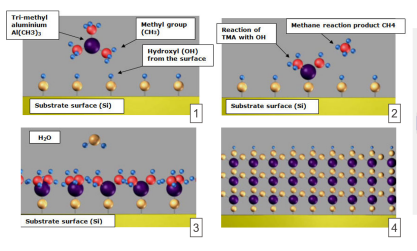
The performance of micro- and nano-mechanical devices depends essentially on the materialsthey are made of. Indeed, the behavior of materials at the nanometer scale can result in differentresults compared to the macroscopic scale. Moreover, in the case of a NEMS-MEMS device usedin a liquid medium, the right selection of materials is imperative to obtain a satisfactory measurement quality: The mechanical domain concerns the resonance properties, the electrical oneis mainly for transduction, where electrodes are used. Indeed, the impermeability at this scaleof the conductive metal parts must be guaranteed for a liquid-purpose device. One suggestedsolution is to consider a passivation layer. The presence of a thin layer of non-conductive material between the conductive parts and the liquid satisfies this role, without considerably affectingthe mechanical properties of the device, nor the electrical properties that are associated withNEMS-MEMS prerequisites. A good candidate is an atomic layer deposition (ALD) of alumina(Al2O3). Its mechanical properties have been widely studied [2]. In order to incorporate itinto the device, its compatibility with clean room microfabrication, which is mainly defined bythe selectivity, must be guaranteed. Therefore, the project focuses on etching properties of theatomic layer deposition (ALD) of Al2O3. For this purpose, etching processes such as plasmaetch with sulfur hexafluoride (SF6), gas etch with xenon difluoride (XeF2), wet etch with MIFdevelopper (726 MIF) as well as ion beam etch (IBE) were performed. Then, the second partof the project focuses on the passivation properties of Al2O3 thin layers. An attempt to studythe passivation of Al2O3 in contact with different liquids (distilled water, acetone, isopropanol)allows to understand more about the electrical modeling and the feasibility of such an approach.A detailed presentation of the experimental setup as well as the phenomena observed are presented as results of the study. This project allows to learn more about the novel passivationproperties of Al2O3 and to incorporate it into NEMS-MEMS for future use.
The project focuses mainly on the microfabrication processes, held in the Center of MicroNanoTechnology (CMi), EPFL. Etching selectivity is an essential criterion to confirm therelevance of using Al2O3 as a passivation layer. Indeed, the release process must not affect thepassivation layer in any way. In addition to that, the device, of which an example of applicationcan be the one detailed in the paper [1], may be composed of a multitude of different materials.Each component has a characteristic thickness that plays a determining role in the mechanicaland electrical properties. To begin with, it is necessary to determine if it is possible to apply apassivation layer of Al2O3 with the atomic layer deposition (ALD) process, at different thicknesses, on materials such as Si and platinum (Pt). The latter is the main component of anelectrode: it must be passivated when the device is used in a liquid medium in order to maintainthe electrical properties unchanged.
There are 4 different etching methods that are studied: plasma etch with SF6, gas etch withthe use of XeF2, wet etch with the 726 MIF developer, and the use of a broad-beam ion etch.The use of SF6 via the equipment AMS200 and of XeF2 thanks to the SPTS Xactix X4 ismainly used for a release process (which allows to etch the silicon wafer in particular), where theselectivity of Al2O3 must be confirmed. The aim is to determine if the etching affects the Al2O3thin layers directly or by the presence of etching byproducts. A summary of the equipment usedthroughout the project is presented in the following table. The parameters to be considered foreach machine, appearing in the process flow 1 and 2, are detailed in the sections dedicated tomicrofabrication and in the results.

Fig1
Then, the next step of the project is the application of Al2O3 as a passivation layer onconductive components of the electrode, composed of Silicon, Silicon oxide (SiO2), Titanium(Ti) and Platinum (Pt). Al2O3 is applied on top of the platinum layer. The final objective is tostudy the passivation properties by the deposition of liquid on the passivated conductive surfaces.For this purpose, a second process flow (named process flow 2) allows the microfabrication ofsuch a design. Then an experimental setup in the laboratory permits to measure the electricalcharacteristics according to a predetermined model. Any electrical change according to themodel is then manifested by the effect of the liquid that has been deposited on the Al2O3, whichplays the role of passivation on the platinum layer. Distilled water, acetone and isopropanol arethe liquids studied for passivation.
To determine the etch rate, the wafer with 96 [nm] of Al2O3 had to be left initially for a certaintime in the developer. Then the thickness after etching is measured with the Filmetrics F54instrument. The difference of thickness after a duration gives an etch rate of 2 [nm/min] ofAl2O3 in the developer 726 MIF. After leaving the wafer for a duration of 60 minutes (includingthe 20% margin), the photoresist had to be rinsed and removed with UFT Remover 1165.