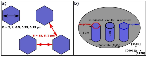
Although GaN etching in Cl2 is driven by ion-enhanced chemical etching mechanisms, the chemicalcomponent is very strong, and Cl2 plasma leads to preferential crystallographic orientation etching of GaN.The mechanisms that drive facet formation are very similar to those involved in wet KOH etching. Theetching ability of a specific crystallographic plane by chlorine atoms depends on the planar density and theN dangling bonds present on the plane. Predictably, GaN crystallographic planes will be etched in Cl2plasmas as follows: a-type semipolar > m-type semipolar planes > a nonpolar plane > m polar planes > cpolar planes. Crystallographic etching usually reveals the slowest etching planes, meaning the m-planes.However, consistently with the wet mechanisms, our study shows that the final revealed plane in Cl2 plasmawill strongly depend on the surface curvature: in concave surfaces, fast-etch facets persist, while in convexsurfaces, slow-etch facets persist. Consequently, Cl2 plasma etching of pillars (convex surfaces) will resultin a-type facets, while etching of holes (concave surfaces) result in m-type facets.
Most promisingly, core-shell light-emitting devices are expected to be a breakthrough development in solidstate lighting [6–9]. In this approach, the emissive quantum wells are grown on the entire sidewalls of thenanowire, which are closely aligned with nonpolar planes. In addition to the advantages of the 3D geometry,this architecture provides: i) an increase in the emissive surface area compared to a planar structure by afactor of about four times the nanowire aspect ratio [2], and ii) an improvement in internal quantum efficiency(IQE) by avoiding piezoelectric polarization and associated electric fields (Quantum-confined Stark effect)through regrowth on high-quality nonpolar facets [10–13].
Therefore, the ability to fabricate organized, dense arrays of GaN nanowires with high aspect ratio is of greatinterest for the next generation of devices, such as core-shell light emitting diodes.The array of GaN nanowires can be obtained through a bottom-up approach (using molecular beam epitaxy[14,15] or metal-organic vapor phase epitaxy [8,9] self-organized growth) or a top-down approach (acombination of lithography and plasma etching steps) [16–20].
The advantage of the top-down approach is that it offers more flexibility in creating arrays of nanowires withdifferent shapes, dimensions, and densities on a wafer scale. However, plasma patterning is known to causedamage and rough surfaces, which prevent high-quality surface regrowth [21,22] while the regrowth of thequantum wells on the nanowire sidewalls for core/shell emitting structures is favored if m-oriented facets arepresent.

The etching experiments were conducted using a Centura 5200 etch platform from Applied Materials, whichcomprises three plasma reactors [29]. First, we thermally glued GaN samples onto a 200 mm carrier waferusing silicone-free thermal paste (Type 1977-DP) from Techspray. Then, we opened the SiO2 hard maskusing Magnetically Enhanced Reactive Ion Etching (MERIE) with an Ar/C4F8/O2 plasma. This plasmaprocess ensures a SiO2/resist etch selectivity of 1.7. Finally, we stripped the resist using an O2 plasma, witha SiO2 carrier wafer being used for both these steps.
For the GaN etching step, an Inductively Coupled Plasma (ICP) reactor (Decoupled Plasma Source, DPS,from Applied Materials) is used with a Cl2 plasma (190 sccm), a pressure of 25 mTorr, a source power of400 W, and a bias power of 140 W (corresponding to a VDC of -450 V). The chuck temperature is maintainedat 55 °C, and a SiN carrier wafer is used for this step. The GaN etching process is monitored in real-timeand stopped at the end of the process using an endpoint system that utilizes interferometry with a Xenonlamp providing wavelengths from 200 to 800 nm (EyeD from Verity instrument). After GaN etching, bufferedoxide etch (BOE) wet solution is used to remove the hard mask layer.
上一篇: 低温蚀刻过程中涉及的钝化机制
下一篇: Al2O3层的蚀刻选择性和钝化性