Most processing of the III nitrides is currently done bydry plasma etching.1,2 There are several disadvantages to dryetching, including the generation of ion-induced damage3and difficulty in obtaining smooth etched sidewalls, whichare required for lasers. The typical root-mean-square ~rms!roughness of sidewalls produced by dry etching is on theorder of 50 nm,4,5 although recently surfaces with an rmsroughness as low as 4–6 nm have been reported.6 Photoenhanced electrochemical ~PEC! wet etching has also beendemonstrated for etching of gallium nitride (GaN).7–10 PECetching has the advantage of relatively low equipment costand low surface damage, but a method for producing smoothvertical sidewalls has not yet been found. Cleaved facets forGaN have also been reported, with rms roughnesses varyingbetween 16 nm for GaN grown on sapphire substrates11 and0.3 nm for GaN grown on spinel substrates.
While KOH-based solutions have been found to etchAlN and InAlN, no acid or base solution has previously beenidentified that is able to etch high-quality GaN.13 In this letter, we have used ethylene glycol, instead of water, as asolvent for KOH and NaOH so that we are able to employtemperatures between 90 and 180 °C. These temperatures exceed the boiling point of water and are considerably higherthan the temperatures used in previous references.13 By sodoing, we have developed a two-step process that etchescrystallographic surfaces into III nitrides. Our samples are 2-mm-thick n-type GaN epilayers grown on c-plane sapphireby metal-organic chemical vapor deposition ~MOCVD!, andthe films have an x-ray diffraction rocking curve full width athalf maximum of ;800 arcsec.
The first of the two etching steps in the crystallographicetching process is used to establish the etching depth, and itcan be performed by several common processing methods.For our first step we have used several different processingmethods, including reactive ion etching in a chlorine-basedplasma, PEC etching in a KOH solution, and cleaving. Thesecond step is done by immersion in a chemical that is ableto crystallographically etch GaN. This etching step can produce smooth crystallographic surfaces, and the specific etching planes can be chosen by varying the orientation of thefirst step, the chemical agents, and the temperature. The etchrates and crystal planes observed for all chemicals used inthis work are summarized in Table I. The etching planeslisted in this table are those that appear during the etch. Because the c plane $0001% is impervious to all of these chemicals except at defect sites where etch pits occur, it is also anetch plane, with a negligibly small etch rate.

Fig1
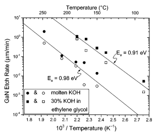
The activation energies for etching in these various solutions is 0.9 eV, or 21 kcal/mol, as inferred from theArrhenius plots in Figs. 3 and 4. Note that this is equal to thecalculated heat of formation of GaN, 0.90 eV.17 The activation energy indicates that the etch is reaction-rate limited. Ifthe etching were diffusion limited, an activation energy inthe 1–6 kcal/mol range would be expected.
It is interesting to note that the etch rate of KOH dissolved in ethylene glycol is higher than the etch rate of molten KOH at the same temperature. In fact, the etch rate as afunction of concentration peaks at a value of 40% KOH byweight in ethylene glycol, as can be seen in Fig. 5. We believe that this is due to high solubility of the etch products inethylene glycol.