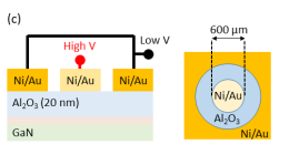
Controlling the plasma etching step involved in MOSHEMT GaN fabrication isessential for device performance and reliability. In particular, understanding the impact ofGaN etching conditions on dielectric/GaN interface chemical properties is criticallyimportant. In this work, we investigate the impact of the carrier wafers (CW) (Si,photoresist, SiO2, Si3N4) used during the etching of GaN in chlorine plasma on theelectrical behavior of Al2O3/n-GaN metal-oxide-semiconductor (MOS) capacitors.
XPS analyses show that the Al2O3/GaN interface layer contains contaminantsfrom the etching process after the Al2O3 deposition. Their chemical nature depends on theplasma chemistry used as well as the chemical nature of the carrier wafer. Typically, Cland C are trapped at the interface for all substrates. In the particular case of Si carrierwafer, a significant amount of SiOx is present at the Al2O3/GaN interface. thecapacitance–voltage characteristics (C–V) of the MOS capacitors indicate that thepresence of Si residues at the interface shifts the flat band voltage to negative values,while the presence of Cl or C at the interface increases the hysteresis. We demonstrate that introducing an in situ plasma cleaning treatment based on N2/H2 gas, before the ALDdeposition, allows the removal of most of the residues except silicon and suppresses thehysteresis.
In the last decade, GaN-based transistors have experienced significant adoptionbecause of their high-power and high-frequency characteristics, along with their capacityto function at high temperatures. Conventional GaN transistors operate in a normally-oncondition (i.e. depletion mode). For high power applications, normally-off devices (i.e.enhancement mode) are preferred because of the circuit simplification and safeoperation1.
Varieties of approaches, including gate recessed2,3, fluorine ion implantation4, pGaN cap layer5,6 have been exploited to achieve the normally-off behavior of GaN-baseddevices. The gate recessed approach is a promising technology since it enables to keephigh mobility and high density of electrons without compromising the voltage threshold.Among the different technical steps used in the GaN recess approaches, plasma etching iswidely employed to control accurately the recessed depth. However, the etching stepmodifies the GaN surface composition (e.g. N-depleted surface, etch residues) and thesurface morphology7,8. The deterioration of the GaN surface necessarily leads to a poordielectric/GaN interface quality. The latter is responsible for an increase in hysteresis,frequency dispersion, and interface density states. Electrical characteristics are commonlycompared regarding different dry or wet etching processes. Wang et al. observed themodification of the electrical characteristics when using different chlorinated-based etching gases9. Vauche et al. showed that the interface composition influences thethreshold voltage on GaN MOS-HEMT10. Jackson et al. observed modification of theinterface composition and the average interface trap density.

Fig1
The etching processes are performed in a 300 mm Centura® Advant-Edge™MESA™ inductively coupled plasma (ICP) etch tool commercialized by AppliedMaterials. More details of the etching tool can be found elsewhere15. During the etchingexperiments, the 1.5×1.5 cm² GaN samples are thermally glued with a thermal paste atthe center of a 300 mm carrier wafer. Several carrier wafers have been used: a bare Siwafer, or a Si Wafer on which either a 1 μm-thick photoresist is spin coated or a 100 nmthick SiO2 is thermally grown or a 55 nm-thick Si3N4 is deposited by Low-PressureChemical Vapor Deposition.
下一篇: 晶圆级单晶金刚石的常用工艺