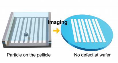
The extreme ultraviolet (EUV) pellicle as a physical shield for the photomask is emerging and becoming essential for the fabrication of nanodevice under 5 nm. The microparticles inevitably exist in the EUV lithography (EUVL) chamber with a hydrogen environment (3 Pa), which can have an unfavorable effect on the formation of fidelity nanopatterns on the processing wafer (Figure 1). Putting a EUV pellicle over a reticle causes the particles to become entangled in the pellicle, and EUV light reflected from the reticle is easily and defect-free delivered to the wafer, while EUV light reflected from the particle is interrupted (outof-focus). ASML, the only supplier of EUVL systems in the industry, outsources the assembly and distribution of these products to a private firm. Others are also developing pellicles for EUV, a sophisticated lithography process at a wavelength of 13.5 nm to pattern sub-10 nm-scale features on wafers.
In order to realize the EUV pellicle, strict criteria must be fulfilled:[1,2] i) EUV transmission of more than 90% [tens of nanometers thick and nonuniformity (3σ) ≤ 0.4%], ii) excellent thermal and chemical stability upon exposure to EUV with a high energy density of 5 W cm−2 (over 400 W), iii) strong mechanical properties (maximum acceleration of 100 m s−2, pellicle moving speed in the EUVL chamber, Young’s modulus over 1 TPa), iv) maximum ambient pressure rate of change (3.5 mbar s−1 ), and v) full-size pellicle (110 mm × 140 mm). Conventional pellicle candidates including Si,[3,4] SiNx, [5] and Si-Mo-Nb multilayers[3] could be easily damaged by EUV radiation because the strong absorption of EUV light happens to all the elements with atomic number Z ranging from 1 to 86[6,7] as well as their low thermal conductivity and emissivity. In addition, as the pellicle is fabricated, the pellicle materials suffer from structural challenges that are freestanding on the frame (110 mm × 140 mm) with tens of nanometers, resulting in cracks or fractures of the pellicle. To satisfy these stringent standards, a breakthrough in pellicle material and transfer process is necessary.
Graphene, which is a single atomic layer containing only carbon atoms with sp2 hybridized chemical bonds, possesses outstanding thermal and electrical conductivity, chemical and mechanical properties, and a protective barrier to isolate metal surfaces, allowing it to be implemented as a pellicle that meets key requirements[1,2] for EUVL pellicle technology. The first step in the growth of large-scale single-layer graphene on Cu foil and multilayered graphene on Ni film/ silicon substrate by CVD technique was to verify the synthetic mechanisms on the self-limiting way[8] in 2009 and carbon solubility of Ni/ carbon precipitation during cooling[9] in 2009, respectively. In the beginning, graphene was mainly utilized for the transparent electrode[10] and graphene field-effect transistor,[11] but there was no technical interest in the pellicle application in EUVL. Furthermore, despite its exceptional strength of 130 GPa (within 1.5 µm diameter of graphene film only),[12] single-layer graphene was too thin to be freestanding on a frame with the whole size of pellicle 110 mm × 140 mm in air. In 2015, the NGF pellicle with 50 mm × 50 mm size was demonstrated for the very first time.[2] At first, the critical issues for realizing NGF pellicle were i) uniform NGF synthesis with lower defect density, ii) conformal NGF transfer on the frame, and iii) large-scale characterization tool development. In this section, we will review the developing synthetic method for NGF pellicles.

Fig1
From this technique, the large-scale (120 mm × 120 mm) NGF with a thickness of 38 nm were directly synthesized at a relatively low growth temperature (870 °C). Still, the thickness of grown NGF is required to be less than 20 nm without any etching procedures if EUV pellicle transmission is to surpass 90%. For the enhancement of NGF uniformity with a thickness of around 20 nm, a CVD technique involving a rapid cooling step and a separate precipitation step before the cooling step was proposed.[21] As long as the increased cooling rate to room temperature (RT) is sufficiently fast (>20 °C s−1 , c.f. conventional cooling rate: 9 °C s−1 ), the carbon atoms are frozen in the Ni, the supersaturated solid solution is maintained, and graphite does not form on the Ni surface at RT. In the separated precipitation step at the relatively low temperature (700 °C), high-density and homogeneous nuclei are formed on the Ni surface without the sparsely grown graphene/graphite nuclei at 910 °C, resulting in improved thickness uniformity and coverage of the NGF (Figure 4d).