A novel wafer-scale silicon fractal fabrication method is presented here for forming pyramids only in the lateral direction using the crystal orientation of silicon. Fractals are fabricated in silicon by masking only the corners (corner lithography) of a cavity in silicon with silicon nitride, where the shape is determined by the crystal {111} planes of the silicon. The octahedral cavity shaped by the {111} planes was previously only used for forming octahedral fractals in all directions, but by using a planar silicon dioxide hard-mask on a silicon (100) wafer, the silicon octahedral cavity is “cut in half”. This creates a pyramid with sharper edges and vertices at its base than those determined by just the {111} planes. This allows selective corner lithography patterning at the vertices of the base while leaving the apex unpatterned, leading to lateral growing of pyramidal fractals. This selective patterning is shown mathematically and then demonstrated by creating a fractal of four generations, with the initial pyramid being 8 µm and the two final generations being of submicron size. Keywords: micromachined fractals; corner lithography; submicron; wet-etching; pyramid.
Fractals consist of broken geometries featuring identical shapes in various scales. In Latin, fractal means broken or fractured and the term was introduced by the mathematician Mandelbrot in 1975 [1]. The concept of fractals has interested many scientists in various fields. In crystalline silicon (Si) micromachining, it has been shown that lateral fractals can be fabricated along preferential crystallographic directions photoelectrochemically with some level of directional control using photoelectrochemical etching [2,3]. However, the fabrication of fractals can be quite labour intensive and complex when making each generation in a controlled manner with respect to orientation and shape. It has been demonstrated that 3D fractals can be engineered in a robust and time-efficient way using corner lithography in combination with anisotropic wet-etching in an auto-multiplying process. The crystallographic nature of Si is used to fabricate smaller features at the concave corners of geometries bounded by the slow etching {111} planes .
The geometry of the residual layer in the concave corners depends on the number ofintersecting planes. Two intersecting planes result in a thin residual "wire" and three ormore planes in a small residual "dot". This defined residual layer can be well controlledif the structural layer is conformally deposited and etched highly isotropic and selectiveIt is compatible with micro- and nanomachining, where the initial template defines theexact position and spatial arrangement. This method was further investigated for using itas an inversion mask in combination of local-oxidation-of-silicon (LOCOS) in subsequentfabrication steps (4,5]. A pyramid with tunable nanoapertures close to the tip was fabri.cated. Furthermore, this process showed to be capable of creating vertical and horizontalsuspended nanowires .

Fig1
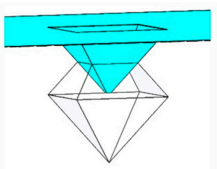
When looking at a basic octahedron, which is defined by the crystalline (111) planesof the Si crystalline lattice (Figure 4), there are two types of corners. Edges are the lineswhere two planes meet, and vertices are the points where two or more edges, or 3 or moreplanes, meet. For an octahedron, all 12 edges have the same angled symmetry, as do the sivertices when the vertices have a smaller angle between opposite planes than at the edges[his means that when an inside-deposited material would be etched from the inside, ittakes longer to etch all the material from the vertices than the edges. This allows for severallevels of controlin corner lithography over selectively addressing corners, as demonstratedby previous work (5,6). By halving the octahedron, a pyramid is obtained, as shown inFigure 4b. This adds sharper edges and vertices at its base, allowing for a selective cornercontrol of four stages.