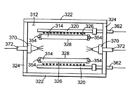
An immersion processing System is provided for cleaningwafers with an increased efficiency of chemical use. Such aSystem advantageously uses less cleaning enhancement Substance that may be provided as gas, Vapor or liquid directlyto a meniscus or wafer/liquid/gas bath interface So as toeffectively modify Surface tensions at the meniscus withminimized chemical usage. Such a delivery System designmay be applied for Single wafer processing or for processingmultiple wafers together within a Single liquid bath vessel.For Single wafer processing, in particular, cleaning enhancement Substance can be delivered along one or both majorSides of the wafer, preferably at the meniscus that is formedas the wafer and liquid are relatively moved, while aprocessing vessel usable for Such Single wafer processingmay itself be designed with a minimized size to accommodate a single wafer. By reducing the vessel Volume, chemicalusage for any processing chemicals that are to be provided within a liquid bath may also be advantageously reduced.
The present invention relates to the wet processing andcleaning of Semiconductor wafers within a liquid bath andthe Subsequent Separation of wafers from the liquid bathwhile cleaning wafer Surfaces. In particular, the presentinvention relates to Separation of one or more wafers froma liquid bath after wet processing while providing a cleaningenhancement Substance to an object/liquid/gas interface forenhanced Surface cleaning.
Wet processing of many types of objects often includes aStep of Separating the object from the liquid as either afinished product or for further processing. Moreover, it isoften desirable to rinse and/or clean the object after wetprocessing to remove any contaminants or left over andunwanted processing liquids and to provide a clean processed object. Also, in many cases, depending on any furthertreatment or handling, the object may be further dried toremove any processing or rinsing liquids that may still bepresent on a Surface of the object.

In the case of processing microelectronic devices, Such asincluding Semiconductor wafers at any of various Stages ofprocessing, flat panel displays, microelectrical-mechanicalSystems (MEMS), advanced electrical interconnect Systems, optical components and devices and components of massdata Storage devices (disk drives) and the like, cleanliness iscritical in Virtually all processing aspects. RepresentativeSteps in wet processing of wafers include wafer etching andrinsing. For processing Such microelectronic devices, it isimportant to use clean processing liquids So as not tointroduce contaminants into the processing environment,and likewise as important to separate the wafer(s) from theliquid bath in a way to Substantially prevent contaminantdeposition onto a wafer Surface, including contaminants thatmay be Suspended within the liquid bath (as potentiallypresent from the processing liquid, the wafer Surface, or asa result of the processing Step).
In this regard, techniques and apparatuses have beendeveloped for rinsing and Separating wafers from immersion(or liquid bath) type processes, and, by Such process or bya Subsequent drying process, to leave wafer Surfaces SubStantially clean. A popular rinsing technique is known ascascade rinsing. Such cascade rinsing utilizes a cascaderinser having inner and Outer chambers that are separatedfrom one another by a partition or weir. Rinse water flowsfrom a water Source into the inner chamber. The innerchamber fills with rinsing liquid until it overflows so thatrinsing liquid cascades over the partition or weir into theouter chamber. Typically, DI water is used as the rinsing liquid, which DI water is preferably rendered extremelyclean, such as by filtering as disclosed in U.S. Pat. Nos.5,542,441, 5,651,379 and 6,312,597 to Mohindra et al.
上一篇: 薄膜 PMUT:40 年研究回顾
下一篇: CMP