The electronics industry has grown rapidly in the past three decades. Ultra-large-scaleintegrated (ULSI) circuits, with 108 or more devices on a chip, can now be fabricated onsemiconductor substrates, or wafers, to reduce cost and to increase the performance ofelectronic products. Figure 1.1 shows the growth of the number of components on a metaloxide-semiconductor (MOS) memory chip. That number has approximately doubled everytwo years over the past two decades, matching the rate Moore forecast (Moore, 1965; Changand Sze, 1996). Concurrently, the minimum dimension of the device-feature continues toshrink by about 13% per year, or by a factor of two every six years, due to the advances infabrication technology. The decrease of feature length reduces the overall device size andincreases the packing density, and thus reduces the cost of function. Moreover, device speed,which varies inversely to feature length, has been improved and power consumption, whichapproximately varies as the square of feature length, has been reduced. On the other hand, thecomplexity of microchip design and fabrication has increased continuously with integrationand miniaturization. Extremely high degrees of repeatability and uniformity are required inwafer fabrication for a high production yield. One challenge is the demand for global surfaceplanarity for the stringent depth of focus of the lithography in the back-end process integration.The surface topography of the inter-level dielectric (ILD) builds up after multiple levels ofmetal wiring. The Chemical Mechanical Polishing (CMP) process has emerged as a criticaltechnique to smooth surface topography. Additionally, new materials such as Cu and W,introduced in ULSI fabrication, also require extensive use of the CMP process to form inlaidinterconnect structures. A fundamental understanding of the CMP process is essential toimprove process optimization and control, and to increase the process yield and throughput inthe continuous integration and miniaturization in the semiconductor industry.
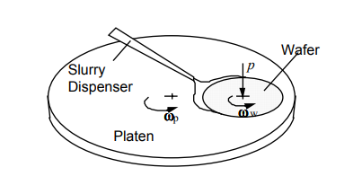
Figure 1.2 is a schematic of a conventional CMP process. It is an adaptation of thelapping technology used to polish plate glass. The wafer to be polished is mounted on a wafercarrier via back pressure or via surface tension by wetting its back surface. The wafer ispressed down against a rotating platen, which holds a compliant polishing pad. The waferslides on the pad surface with a relative velocity generated by the rotation of the carrier andthe platen. Concurrently, the abrasive slurry drips onto the platen surface and dispensesthrough the wafer/pad contact interface. The chemical slurry and abrasive particles retainedon the porous pad surface remove the material on the wafer surface.
There are two major applications of CMP in ULSI manufacturing: to smooth surfacetopography of inter-level dielectrics (ILD, usually silicon dioxide), or to remove excessmaterial to produce inlaid metal structure or isolation trenches. The inter-level dielectricCMP is applied in conventional aluminum metallization, where aluminum is deposited on theoxide ILD layer, patterned, and etched to form interconnects. Another layer of oxide is thendeposited to insulate the aluminum interconnects. Thus three-dimensional electrical wiring isconstructed. Device elements, such as resistors, capacitors and transistors, are connected tobuild up ICs. In this practice, CMP is employed on at least the top few layers of each ILDsurface to provide a smooth surface for aluminum deposition and to provide a field flatenough that contact vias and metal wires can be patterned by lithography. The desired processend-point is determined based on the surface planarity and the thickness of the ILD layerrequired for electrical isolation of aluminum line. Figure 1.3 (a) shows the schematic for theILD CMP. Wafers stacked with three or more layers of aluminum interconnects, such as areused in microprocessor applications, are usually subjected to ILD CMP to improve yield andreliability.

Fig1
The original commercial practice of CMP inthe semiconductor industry was to prepare raw silicon wafers. After the wafer was sawedfrom a single-crystal silicon rod, the mechanically damaged surface layer was removed andthe surface planarized to produce a flat, scratch-free surface for VLSI devices and circuits.Monsanto first developed this process and sold polished wafers in late 1962 (Walsh andHerzog, 1965; Hippel, 1988). Despite its recent use in VLSI fabrication, the polishingprocess has been employed for optical lens fabrication for centuries. In fact, the firstmachinery used by Monsanto was very similar to the commercial machine used in the opticalindustry. Monsanto’s innovation was to redefine the polishing steps and choose properpolishing abrasives and slurry chemicals to achieve the specifications for both surface finishand planarity of silicon wafers. By using submicron silicon dioxide abrasives in an alkalinesolution, the process time was reduced from one and a half hours to about five minutes.
Due to the fast shrinkage of the feature size and theincreased number of devices, more metal-interconnect layers were required for each newgeneration of ICs, especially for logic chips and microprocessors. The quick build-up ofsurface topography with the increase of interconnect layers usually results in a poor stepcoverage of the metal deposition. It thus requires a global planarization technique on the ILDsurface. The smaller wavelength light employed in lithography to produce submicron featuresalso sets a more stringent limit on surface planarity. The superior ability of CMP to produce aflat and smooth surface provides an ultimate solution for more complex chip design. Keepingthe CMP performance robust and reliable became a key issue for integration of the CMP intothe large-scale manufacturing operation. In 1993, Intel demonstrated intense use of CMP onthe new three-level microprocessor, the Pentium chip. It was the first time that CMP wasemployed to produce high volumes of commercial devices.
上一篇: 半导体晶片清洗系统和方法
下一篇: 磷酸蚀刻增强纳米坑TiO 2表面亲水性