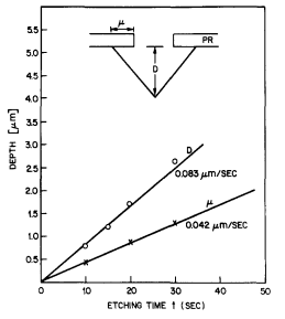
A photoresist etch mask process has been developed for the etching of (110) direction, (111B) faceted v-grooves in InP(001) wafers. Etching rates are measured about 0.083 and 0.042 ~m/s for etching depth and undercutting, respectively. Theundercutting mechanism is discussed. The deterioration of the etching solution and the resist mask have been studied.
Chemical etching of III-V compound semiconductingmaterials plays an important role in optical-electronicdevice technology. Important factors determining thechoice of an etchant are the etching rates of the materialsin the system, the solution chemical aggressiveness toward etching masks, the desired etching profile, and thedegree of surface quality and undercutting.
A number of investigations have been made on theetching characteristics of InP crystals. Adachi (1) has developed a new etchant system, HBr:CH3COOH (H3PO4):K._,Cr2OT, for fabricating InGaAsP/InP mesa-shapedstructures. Kambayashi et al. (2) have developed anothernew etchant system, HCl:CH3OOH:H202, for fabricatingInGaAsP/InP etched-mirror lasers and integrated optical circuits. Adachi et al. (3) have reported etching characteristics of InP in the Br2:CH3OH system. Phatak et al.(4) have reported on the etching characteristics of InPusing HCl:H3PO4 solution. However, they have not reported the fabrication of v-groove structures on InP substrates and such structures are important for laser diodeapplications.
As received InP (001) oriented wafers are cleaned by aconventional chloroform acetone-methanol (CAM) solvent clean, rinsed in distilled water, blown dry with highpurity nitrogen, etched in HF to remove native oxide,blown dry with high purity nitrogen, and then prebakedat 120~ in air for 25 rain. A positive photoresist (Microposit 1400-23) is spun onto the sample and softbaked at90~ in air for 25 min. The photoresist thickness isaround 1 ~m. The PR etch mask is direct contact patterned with a Karl Sflss aligner and 1.0 ~m mask to openup 1.0-1.7 ~m wide windows, aligned parallel to the<011> crystal direction. The exposed wafer is then developed in Microposit developer. After a 120~ hardbakefor 25 min the wafer is etched in a 3:1 HCl:H3PO4 mixedetchant at room temperature. This process involvingCAM (organic solvent) clean-H20 rinse-HF etch-H20rinse-120~ prebake-PR spin-90~ postbake-expose-PRdevelop-120~ postbake-3:l etch will, for convenience ofreference, be referred to as the "standard process." Afteretching, the {110} plane perpendicular to the etchedchannel direction is cleaved. Etching profiles are examined by using an AMRAY scanning electron microscope(SEM) with a sputtered Au coating on the photoresist.
To evaluate the degradation of the 3:1 etching solution,photoresist masked wafers were sectioned into fourpieces and etched in the same solution which was storedin an open mouth beaker at room temperature for various times. Figure 5 shows the etching profiles of (001)InP etched in the 3:1 etchant (a) fresh prepared, (b)22.75h old, (c) 93.75h old, and (d) 164.5h old. Figure 6shows the time dependence of the etch factor in the 3:1etchant. The etch factor has the same value after 22.75hand then increases dramatically with time. These data indicates that the etching solution can be stored in an openmouth beaker at room temperature for 20h withoutshowing any significant degradation in v-groove etchingprofiles. The deterioration of the etching solution may bedue to the loss of the HC1 gas from the solution. Figure 7shows the etching profiles of (001) InP etched in the 3:1etchant after photoresist was applied for (a) one week, (b)two weeks, (c) three weeks, and (d) four weeks. All ofthese four wafers were cleaved from the same largephotoresist-coated wafer and stored in air before etching. The time dependence of the etch factor is shown inFig. 8. The results show that the photoresist-coated wafers can be stored in air for at least one week beforeshowing any significant deterioration in v-groove etching profiles.

Fig1
Concentrated HC1 etched InP at a very fast rate (-0.2~m/s in the <100> direction at 67~ This etch rate canbe reduced by the addition of H3PO4 (4). Figure 9 showsthe etch factor on the (001) plane as a function of H3PO4content at 67~ Percentages quoted are by volume. Theetch factor decreased with increasing HC1 concentrations up to 83% HC1 by volume. This result indicates that,at the higher HC1 concentrations, etching is more preferential; the undercutting of InP is slower compared withthe etch depth.