Transmission X-ray microscopy (TXM) is an imaging technique that bridges theresolution gap between visible light microscopy and electron microscopy. Today,synchrotron-based soft X-ray microscopes allow a resolution down to 10 nm, and laboratoryX-ray microscopes, usually operating in the multi-keV photon energy range up to 8 keV,enable a resolution of about 50 nm. Since photons in the X-ray energy range are able topenetrate deep into the object, X-ray imaging is characterized by a samplethickness / resolution value of ~ 103(see Figure 1.1 [Kut+22a]), which is a ratio that allowstomography. That means, nano X-ray computed tomography (nano-XCT) is a uniqueanalytical technique for non-destructive 3D imaging of the interior of objects or materials withhigh spatial resolution. In contrast to X-ray microscopy, visible light microscopy providesusually 2D images, and electron tomography in the transmission electron microscope (TEM)requires the preparation of small samples with a lamella thickness in the ~ 100 nm range.
The unique capability of the nano-XCT technique to image the interior of opaquesamples non-destructively with sub-100 nm resolution is a necessary condition for the studyof kinetic processes in objects and materials. The high-resolution imaging of microstructureor morphology of materials provides valuable information to materials science andengineering, particularly for the design and for the synthesis of new materials. The study ofkinetic processes in systems (e.g. microchips, battery electrodes) delivers essential information for solid-state physics, chemistry and fracture mechanics. Nowadays, 100 yearsafter Griffith’s ground-braking paper describing the fundamentals of fracture mechanics[Gri21], mechanical properties of materials in micro- and nanoscale dimensions have becomean important area of fundamental research in solid-state physics and materials science,including the development and introduction of new techniques for micro- and nanomechanicaltesting [PWK18, Ast+19]. At the same time, there is an increasing need of industry to evaluatethe risk of microcrack evolution at small length scales since crack growth can causecatastrophic failure in 3D-nanostructured systems and functional materials such ascomposites, battery electrodes and integrated circuits (ICs).
Targeting on engineered damage-tolerant 3D-nanopatterned structures, a novelmethodology for controlled crack steering into regions with high fracture toughness and fordetermining the local critical energy release rate Gc for crack propagation in 3D-patternedsystems is developed and applied in this thesis. Nanopatterned on-chip copper interconnectstructures of advanced microchips, insulated by organosilicate glasses, were chosen as anexample system to study fracture effects on small scale, since this a well-defined 3Dnanopatterned system and since a high mechanical robustness is required for microchips. Thecombination of micromechanical testing and high-resolution X-ray imaging opens the way forthe development of design concepts for novel engineered materials systems based on theirlocal mechanical properties.
Mechanical failure caused by microcracks that were introduced into a microchip duringthe manufacturing process, e.g. during dicing of a semiconductor wafer, are a seriousreliability concern for microelectronic products [Kut+22a]. The risk of microcrack growth andeventually fracture in the backend-of-line (BEoL) stack has been increased since theintroduction of so-called low-k and ultra-low-k (ULK) materials – with low dielectricpermittivity but also low Young’s modulus and cohesive strength, and consequently lowfracture toughness - to insulate the on-chip metal interconnects. These effects have beenfurther pronounced by new manufacturing technologies (thinned silicon, advanced packaging)and – since these are mainly thermomechanical effects – by the materials used having differentcoefficients of thermal expansion (CTE). The integration of materials with different CTEvalues results in mechanical stress caused by thermal processes during the microchipmanufacturing – both BEoL manufacturing and (advanced) packaging - and during operation.

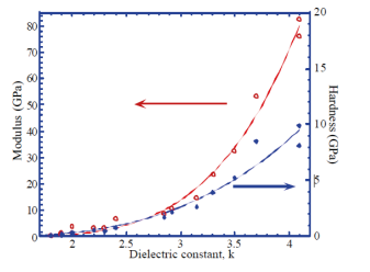
Hence, it can be seen that with an increase of stress σ due to material properties mismatch(Table 2.1) and with a decrease of Young’s modulus E for low-k materials (Figure 2.1), therisk of crack propagation in the BEoL stack is dramatically increased. Typical failure modesare delamination along dielectrics interfaces (adhesive failure) and fracture in dielectrics(cohesive failure). Delamination can be caused by micro-cracks that were introduced duringmanufacturing, for instance during the mechanical dicing process [Bak+12]. To improve thefracture behavior of the integrated BEoL structures, a mechanically robust patterned metalstack against fabrication and packaging stresses is required.
The design of on-chip interconnects, and particularly of GR structures that aremechanically robust against packaging stress, and the evaluation of the risk of mechanicalfailure require the understanding of the kinetics of the fracture process, the identification ofweak structures in the BEoL stack and quantitative measure of fracture resistance, e.g. Gc,under realistic and controlled loading conditions. Li et al. demonstrated a method to controlcrack propagation in Cu/low-k BEoL stacks and to extract the fracture properties of metal viasand interlayer dielectrics from integrated structures [Li+13]. This experimental approach isbased on a double cantilever beam (DCB) test with various specimen geometries, includingsymmetric and asymmetric configurations (mode mixity), and post mortem scanning electronmicroscopy (SEM) and transmission electron microscopy (TEM) imaging of the crack path.
上一篇: 一种新颖的蚀刻掩模工艺