The stable, long-term functioning of devices based on 2D materials is one of the main challenges toward their technologicalapplications.[1] The transport properties of graphene field-effecttransistors (GFETs) on a gate dielectric such as silicon oxide arestrongly influenced by exposing to ambient conditions due tothe adsorption of ambient adsorbates such as water, resultingin undesirable p-type doping.[2–4] This uncontrolled doping results in the device-to-device variation of the transport properties, which prevents their reliable applications in, e.g., the GFET based sensors.[5] Another possiblesource diminishing the performance ofGFETs is the polymer residues on thegraphene surface, which can arise fromgraphene transfer or microfabricationof devices. One of the commonly usedpolymers here is poly(methyl methacrylate) (PMMA) used as a support layerduring the transfer of 2D materials[6] aswell as an e-beam resist in lithographyprocess.[7] While acetone cleaning istypically used to dissolve the majorityof the PMMA coating, some residuesinevitably prevail on the surface.[8] Theseresidues serve as a dominant source ofdoping and scattering of charge carriers,thus degrading the electrical properties of devices based on 2Dmaterials.
Conventional techniques for surface cleaning of bulk materials such as plasma cleaning cannot be employed to clean2D materials, as they would etch them or introduce defectsand unwanted chemical groups.[11] Other specific cleaning techniques have been developed in recent years[12] such as thermal annealing in vacuum or H2/Ar environment,[13,14] currentinduced cleaning,[15] laser cleaning,[16] low-density inductivelycoupled plasma,[17] ultraviolet (UV) ozone treatment,[18] wetchemical cleaning[19–22] and mechanical cleaning via in situ electron microscopy[23] or atomic force microscopy.[24,25] Nevertheless, they suffer either from slow processing or need for complicated equipment, the use of harsh chemicals, and in some caseslack of scalability and reproducibility. Therefore, there is a highdemand for more straightforward approaches that are compatible with large-scale manufacturing and environmentally friendly.
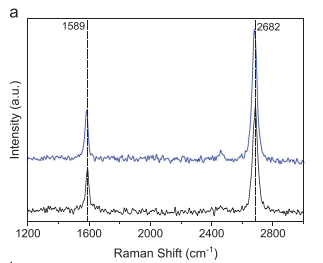
Supercritical fluids (SCF) exhibit a unique combination ofliquid-like density and gas-like transport properties.[26] Above thecritical point, the fluid surface tension is equal to zero while itsdissolving and pores penetration capability remarkably increasethanks to its low viscosity and high diffusion coefficients.[27] Suchphysico-chemical characteristics make SCFs a suitable alternativefor organic solvents in a wide range of industrial and laboratoryapplications. Moreover, SCFs are commercially employed in extraction and purification technologies, namely refining of cooking oils, decaffeination of coffee, etc.[28,29] Carbon dioxide (CO2)is the most commonly used SCF due to its easily achievable critical point state, non-toxicity, nonflammability, and recyclability.[30]Supercritical CO2 drying is widely used to dry delicate biological specimens while preserving their original morphology[31] andalleviate stiction problem in microelectromechanical (MEMS) devices.[32,33] In this work, we show that CPD technique can beused as a robust cleaning/drying postprocessing method to enhance the electric properties of GFET devices. We find that CPDenables enhancement of the field-effect mobility and recovery ofthe undesirable p-type doping of the GFET devices. Moreover,based on the analysis of multiple identical devices, we demonstrate how their functioning is diminished by exposure to ambient conditions, but it can be recovered via the CPD treatment. Wecomplement the detailed analyses of charge transfer characteristics of the samples with morphological and structural characterizations with atomic force microscopy (AFM), X-ray photoelectron spectroscopy (XPS), and Raman spectroscopy. Our findingsshow CPD treatment of graphene-based devices as an effectivestep for achieving their better transport characteristics, which canbe readily integrated into the microfabrication in cleanrooms aswell as on the large scale.
The GFET devices were prepared using CVD-grown graphenetransferred via a PMMA-assisted wet transfer onto a heavily pdoped silicon wafer with 300 nm thickness of thermally grownSiO2. Figure 1a shows the optical microscope image of a chiparea containing 15 microfabricated two-terminal GFETs with anactive area of 190×100 μm2 each, see also a high-resolution optical image of an individual device in Figure 1b. The schematicof a device with the measurement configuration is illustrated inFigure 1c. To collect the field-effect response of each device withthe channel aspect ratio L/W = 1.9, the source-drain current Idsis measured as the function of the back-gate voltage Vg by applying a bias Vds = 10 mV between the source and drain. Figure 1drepresents the exemplary Ids-Vg transfer curves of a GFET devicebefore and after the CPD treatment. The device initially showeda high p-type doping state with a Dirac point at 42 V, which shiftsto near 0 V after the CPD treatment. Furthermore, the transfercurve becomes steeper implying an enhancement of the chargecarrier mobility of the GFET device. The electron-hole conduction asymmetry is remarkably reduced, which denotes the reduction of donor impurities that scatter the electrons more effectivelythan holes.[34,35] Note that contact materials can also contributeto the asymmetry in electron and hole conduction,[36] however,they are not influenced by CPD treatment. The hysteresis (difference of Dirac points in forward and backward gate voltagesweeps) is significantly reduced (see Figure S1, Supporting Information) as well, in average from 33.1 ± 4.9 V to 12.9 ± 3.1 V(Figure 1e). The decreased hysteresis in CPD-treated GFETs indicates a corresponding decrease in the accumulation of chargesin trap centers.[37] These trapped charges are typically caused bybound water molecules on the SiO2 surface, which are screeningthe electric field generated by the back gate.

In summary, we demonstrate the employment of CPD techniqueto GFETs as an effective cleaning/drying post-processing methodto enhance their mobility and reduce their uncontrolled p-typedoping level after microfabrication. Surface analyses confirm thatthe polymeric residues on the graphene surface can be remarkably removed by subjecting the devices to the supercritical CO2in the CPD treatment. Moreover, charge scattering and dopingdue to the adsorbed moisture in the GFETs can be significantlymitigated due to the strong drying upon the CPD treatment. Thistechnique is expected to be promising for future device application based on various 2D materials owing to its simplicity andlack of any toxic byproducts.