The influence of the Nd:YAG laser’s oscillation energy on creating textured surfaces on silicon wafers is investigated in this study. The silicon wafer surfaces were directly ablated by a pulsed Nd:YAG laser beam to create thetexturing, which was then examined using UV–Vis spectroscopy, AFM and FESEM to determine its characteristics. The reflectance was reduced up to 15% after laser texturing of multicrystalline silicon wafers. The siliconsurface suffers from structural defects and a laser damage layer as a result of the laser texturing process, which inturn has an effect on the lifespan of the photo-generated carriers. To compensate for the laser damage layer, thesilicon surface was cleaned with diluted KOH (15%) to remove undesirable particles and the oxide layer. Surfaceroughness and reflectance in silicon solar cells were changed depending on the laser oscillation energy utilizedfor texturing. The roughness and reflectance were measured using AFM and UV–Vis, respectively. The laseroscillation energy of 84 J/p had the highest average roughness of 0.2104 m and the lowest reflectance of 5%. Asa result, standard silicon solar cell devices revealed photovoltaic conversion efficiencies of roughly 7.5% and5.0% for laser-textured grid and one-dimensional line patterns, respectively.
The photovoltaic (PV) industry manufactures solar cells using multicrystalline and monocrystalline silicon wafers. Almost 90% of the silicon wafer substrates are utilized in the PV industry. Silicon (Si) is apopular choice for use in solar cells due to its excellent properties as acheap, abundant element in the Earth, and highly efficient semiconductor. To be noted, crystalline silicon (c-Si) cells are made of siliconatoms that have been interconnected to create a crystal lattice. Thislattice is an organized structure that makes the process of turning lightinto electricity more efficient. There are three requirements that need tobe met before a silicon wafer is used for solar cells. One is that the Siwafer must have a finely defined quadrangular shape and a good surfacemorphology. The other two requirements are a good quality microstructure and low-end impurity concentrations in the Si wafer [1]. Good surface morphology by enhancing the silicon wafer surfaces is verynecessary due to the high refractive index of crystalline silicon (η = 3.4at 550 nm) in the solar spectrum region of 300–1100 nm which createslarge optical losses [2,3,4]. Therefore, texturing of crystalline silicon (cSi) has been utilized to overcome this optical loss by trapping light forthe high efficiency c-Si solar cells. Texturing is employed to reduce thesilicon surface’s light reflectance, thus can enhance light trapping whereit can trap more photons by giving multiple times of photons to absorbinto the silicon wafer substrate, and then improve the short circuitcurrent and solar cell efficiency [5].
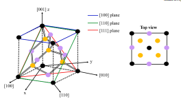
Several approaches, such as texturing Si wafers with dry or wetetching methods or fabricating antireflective composite thin films, havebeen developed [6,7,8]. Due to different grain orientations within thesame wafer, alkaline etching can’t be used to texture multicrystallinesilicon. This is because different grains etch at different rates, which would make the surface uneven. Since it is simple to texture monocrystalline silicon wafers with [100] orientation using an alkalineetchant, such as potassium hydroxide (KOH), they are the most popularsilicon wafer type in the PV industry. As seen in Fig. 1, silicon crystallizesin the form of a diamond cubic lattice, which is formed by two interpenetrating face-centered cubic lattices. In Fig. 1, the blue line denotesthe [100] plane, the green line signifies the [110] plane, and the redline represents the [111] plane.
Surface modification through laser technology interaction can beconsidered as an alternative for reducing the light reflection on Si wafersurface. For more than ten years, laser processing has been used in theproduction of solar cells. Laser technology is utilized in photovoltaicmanufacture for annealing, scribing, texturing, and drilling [9]. Manytypes of laser technology were utilized based on various approaches.Diode-pumped lasers [10], Continuous Wave (CW) diodes [11], femtosecond lasers [12], picosecond lasers [13], and ultrafast lasers [14] are afew examples of the lasers that have the ability to create a texture onsilicon solar cell surfaces. Laser technology usually provides more advantages due to the non-contact between the tools and work specimensand also no tool wear when conducting laser systems [15]. Therefore,laser technology is a popular choice in PV manufacturing.

Fig1
In this paper, a pulsed Nd:YAG laser system is used to show how thesurface of a multicrystalline silicon substrate can be textured. Specialattention has been made in adjusting process parameters such as oscillator energy to texture the Si wafer surfaces due to insufficientresearch information from the other study reports about optimization ofpulsed Nd:YAG oscillator energy and its impact to the Si wafer surfaces.After the surface was treated with a laser, a spectrophotometry system(Lambda 950 UV/Vis/NIR spectrophotometer brand PerkinElmer) wasused to measure the optical reflectivity. The Field Emission ScanningElectron Microscope (FESEM) Model:SUPRA 55VP brand ZEISS is usedto characterize the Si surface morphologies while an Atomic Force Microscope (AFM) with tapping mode was used to study the surface topologies and surface roughness of the Si samples. Furthermore, thecorrelations between oscillator energy, laser scan speed, Si surfaceroughness and the value of the Si surface reflection in the making ofsolar cells are also been discussed.