The development of silicon devices, circuits, and systems in most casesrelies on the wet-chemical etching of silicon wafers (SWs). To achieve deepetching and micromachining, shaping, as well as cleaning, the dissolutionof silicon using liquid chemical solutions is imperative. This study reportsan experimental investigation of surface texturing of silicon wafers using amixture of aqueous potassium hydroxide (KOH) solution and isopropylalcohol (IPA) as a complexing agent to enhance light absorption and reducethe optical reflectance in the visible spectrum. Crochralski (CZ) siliconwafers of 100 mm diameter, 2” <100>-oriented, n-type, resistivity (Ωcm)of 7-21, with polished and lapped surfaces were utilized in the experiment.The process variables investigated included temperature (60 – 90) °C,duration of etching time (30 – 60) mins and concentration of KOH and IPAof (1 - 4) mg/l for KOH and (2 – 8) mg/l for IPA. The properties of the etchedand unetched silicon wafers in terms of morphology, structure,photoluminescence, and electroluminescence were investigated todetermine the effects of the process parameters on the efficiency andstructural properties of the textured wafers. The SEM measurementsrevealed the presence of localized roughening pyramidal images. Thisshowed that the use of KOH and IPA solutions on the silicon wafers revealedpyramidal structures that can be used to control the optical reflectance ofthe silicon wafers due to light scattering by the localized roughening. Theapplied etching procedure also produced low-reflecting materials whosereflectivity increases with wavelength. This study shows that texturedmaterial has great potential in optoelectronic device manufacturingprocesses.
In several studies [12 -14], it was indicated that the nature and amount of IPA and the complexingor wetting agent (KOH) used determines the uniformities and sizes of structures (pyramidal) formed.Additional studies revealed that the IPA concentration had a strong effect on the surface roughnessof <100> -single crystals at 80 ℃ with optimal KOH: IPA concentration of 2:4 [11, 12]. However,the influence of surface texturing on the light-trapping properties of silicon wafers has beenseverally investigated [13, 15 – 17]. Results showed optimum parameters for temperature, etchantconcentration and time with reasonable values for surface roughness, and comparative opticalreflectance in the visible spectrum of less than 10%. In their study, Fashina et al [5] investigated thesurface textured of silicon substrates. The inherent study showed a surface with an averageroughness of 593 nm using the optically textured silicon wafer. This result was in agreement withother studies conducted by Dobrzanski and Drygala [8] and Salwa et al [18]. Furthermore, analyticalmodels were developed to investigate the optical reflection behaviour of alkali-textured SWs undera non-normal incidence angle [19, 20]. Consequently, it was observed the reflectance angles werereduced more at lower angles of incidence, when compared to those on flat substrates. The resultwas in accordance with other earlier studies in literature.
Mechanical and chemical processes are often used in the preparation of polished silicon waferswhere the silicon single-crystal ingots are sliced into circular disks referred to as wafers and thenflattened using the process of lapping which involves scrubbing the wafers with abrasive material[21]. Etching is used to remove any mechanical damage which occurs during the mechanicalshaping processes. Most often, etching process precedes other unit operation processes such aspolishing and cleaning before device construction activities. Chemical etching of SWs is oftenachieved by bathing the wafers in an etchant which could be an acidic solution of HNO3 + HF andKOH [11, 15]. One of the several factors considered in the reduction of the conversion efficiencyin crystalline silicon solar cells is optical losses which are mainly due to surface reflection. Inmitigating this challenge, anti-reflection (AR) and surface techniques have been developed.Consequently, texturing process is undertaken to improve surface morphology for reflectancereduction. Most often, alkali hydroxide etchants such as KOH or NaOH have been used for surfacetexturing of crystalline SWs. These etchants are mixed with alcohol additives which produceanisotropic etching properties that cause orientation difference between the <100> and <111>planes. These etching mixtures give rise to changes in the etching rate, as a result, random pyramidsare formed by the intersection of the <111> planes and aligned to <100>. The most popular solutionused for texturing process is KOH mixed with isopropyl alcohol (IPA) [5, 11, 15]. In semiconductorindustries, anisotropic etching using alkaline solutions at high temperatures is often employed topattern single-crystal SWs. Characterization of SWs of different crystalline orientations and dopingdensities using etching processes have severally been investigated.
To enhance the efficiency of silicon solar cell (SC) technologies, surface texturing of the crystallinesilicon system is necessary [9]. The application of alkaline solutions of either NaOH or KOH andIPA is highly preferred and common for anisotropic etching of crystalline-SWs [15]. Etching atextured surface of microscopic pyramids on SWs with <100> - oriented surfaces have beenimplemented with relatively mild alkaline solutions whose concentration is below 5% using eitherKOH or NaOH. In solar cell developments, the textured surface finds application in theminimization of reflection losses from the front surface to enhance optical light-trapping within thesilicon cells that possess reflective back surfaces.
Surface texturing of silicon wafers using chemical processes has not been adequately characterizedas much as those implemented for thinning in the semiconductor industries. Generally, alkalisolutions, such as KOH or NaOH, have been often applied to the surface texturing of crystallinesilicon systems [24]. Other alkali solutions, like LiOH, CsOH and NH4OH, have also beenreportedly used similarly in literature [24]. To produce a different orientation between the <100>and <111> planes, the various alkali solutions are mixed with an appropriate chemical (alcohol)addition [5] Etching with such a combination brings about a modification in the etching parametersand, consequently, enhances the surface properties of the silicon system. The surface texturing ofSWs could improve the absorbance characteristics which in turn, increase the photo-conversionefficiencies of the cells.

Fig1
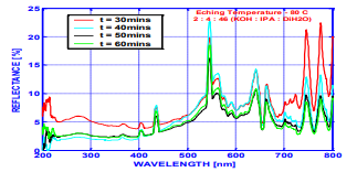
Figure 4 shows the dependence of the reflectance of the textured wafers on the etching time. It wasobserved that the reflectance decreased as the etching time increases reaching an optimum value at40 min etching time. Further increase in time beyond this optimum time has no significant effect onthe reflectance as shown in Figure 4.