The chemical vapor deposition (CVD) of undoped and doped silicon-based dielectric layers plays akey role in the microelectronics technology. To advance the dielectric-layer-related aspects of thetechnology, facilitating its evolution beyond its current level of integration, advanced, lowtemperature CVD processes will be needed. The processes should produce dielectric layers withminimal substrate heating (preferably lowering the "thermal budget"), have no deleterious effectson underlying gate oxides and other device structures, be suitable for filling sub-half-micron highaspect-ratio device and circuit structures, and have reflow characteristics that facilitate the use ofthe chemical-mechanical polishing (CMP) used to achieve planarization. Additionally, they shouldrequire fewer process steps, thereby reducing overall fabrication costs .
At present, Al(Cu)-based conductor films and silicon oxide dielectric films deposited by CVD areused to produce most of the interconnections on multilevel integrated-circuit chips. To facilitate theevolution to higher levels of performance, a significant next step is underway: replacement of theAl(Cu)- based conductors with lower-resistance Cu-based conductors (see for example [2, 3]). Thischange reduces the RC interconnection delay significantly--by a factor of about 1.5. At present, itappears that to achieve a further significant reduction, it will be necessary to reduce the dielectricconstant k of the dielectric films. It is estimated that the delay could be reduced by a factor of about3 if the silicon oxide films, which have a dielectric constant of around 4, could be replaced by filmshaving a dielectric constant of 2 [3]. There is, however, no clear indication of what approach shouldbe used to achieve a reduction in k. One approach, leading to a small reduction (to a value of 3.3-3.5), involves the incorporation of a small amount of bonded fluorine in silicon oxide filmsdeposited by HDP CVD to form a fluorinated oxide. The approach, discussed in detail in this paper,should require only a minimal change in integrated-circuit fabrication [3-7]. Other approaches,leading to a reduction of k to 2-3, involve the use of films such as carbon-doped silicon oxide [8, 9],and carbon and fluorinated carbon [10-16], deposited by either CVD or HDP CVD.
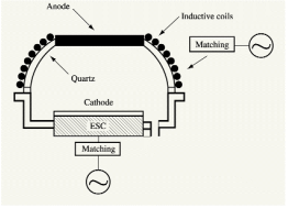
Several commercial high-density plasma CVD systems [32, 35, 36] have been developed inconnection with efforts to advance the integrated-circuit technology to the ULSI (ultralarge-scaleintegration) level. These systems use either ECR or ICP sources for high-density plasma generation.The advantages of each type of plasma source have recently been a subject of extensive discussionsand are not covered here. Readers interested in these plasma sources, which are used in depositionand etching, may obtain more detail from recent publications [17, 18]. Since the commercial ECRsystem has been available for almost ten years, and deposited films and processes have been studiedextensively by this author and many others [19-22, 36-38], we do not discuss additional ECR CVDresults here. In this paper, the emphasis is on recent results obtained for low-temperature HDP CVDof silicon oxide and fluorinated (fluorine-doped) silicon oxide dielectric films, deposited incommercially available inductively coupled plasma (ICP) HDP CVD systems. Results for low-kdielectrics such as carbon and fluorocarbon deposited by HDP CVD processing are also discussed.The promising results obtained lead us to believe that HDP CVD processing may become importantin the future fabrication of integrated circuits.

Fig1
We have used analysis techniques such as Fourier transform infrared resonance (FTIR), Auger,secondary ion mass spectroscopy (SIMS), and nuclear reaction analysis for hydrogen [49] toanalyze the film's bonding structures and composition. A Perkin-Elmer 1725X FTIR system wasused to analyze the films, as described in our recent publication [50]. Auger analysis was performedon a Perkin-Elmer Model 650 scanning auger microscope with a beam voltage of 5 kV and anapproximate current of 100 nA (rastered 100-µm spot size). Other film properties such as stress,wet etching, and CMP rate in conventional oxide slurry were also evaluated.