Purpose The life cycle assessment of silicon wafer processing for microelectronic chips and solar cells aims toprovide current and comprehensive data. In view of thevery fast market developments, for solar cell fabrication theinfluence of technology and capacity variations on theoverall environmental impact was also investigated and thedata were compared with the widely used ecoinvent data.Methods Existing material flow models for silicon waferprocessing for microelectronic chips and solar cells used forengineering and planning formed a starting point for thisanalysis. The models represent an average of widely usedprocesses and associated process equipment. The resultinginput/output tables formed the data basis for the life cycleassessment. This is a cradle-to-gate investigation, consistingof primary gate-to-gate data for wafer processing. Theupstream processes of the necessary inputs were supplemented with data from ecoinvent v2.0. Subsequent manufacturing steps, utilization, and waste disposal of the finalproducts were not included. The software used for creatingthe inventory and impact assessment was Umberto version5.5. The Impact 2002+ method was applied for impactassessment.
Results For both semiconductor and solar cell fabrication,energy consumption and upstream chemicals production aremost relevant for the overall potential environmental impactwhen only the gate-to-gate processes are considered. Theupstream process for wafer production is dominant in solar cellfabrication, but exerts little influence on semiconductorfabrication. In the case of semiconductor fabrication, acomparison with the present ecoinvent dataset “wafer, fabricated, for integrated circuit, at plant” shows large differences.Conclusions In the case of silicon solar cells, the results ofthis study and the ecoinvent data are very similar and theimpact of different fabrication processes appears to be minor.
Processing crystalline silicon and using the semiconductingeffect form the basis of both industries. Processes ofsemiconductor fabrication are also found in solar cellfabrication, although processing microelectronic wafers ismore precise. In crystalline silicon solar cell productiontypically five to seven process steps are applied in a linearsequence to the bare wafer, before the processed wafer is cutand used to build-up photovoltaic modules. Whereas inmicrochip fabrication there are up to 400 process steps beforethe array of microchips on the silicon wafer is finished and canbe cut, packaged, and bound to electrical connections. These400 process steps are run in about 12 specialized process areas,which require the wafer to circulate in the area of production.The different structure of production results also in verydifferent times required to complete production (“cycle time”).

Fig1
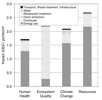
The impact assessment results show that environmentaldamage for 1 m2 fabricated DRAM and logic wafer isdominated by energy consumption in almost all categories,followed by the upstream production of chemicals (Figs. 1and 2). In the chemicals sector, the utilization of nitrogenmakes the largest contribution. As regards ecosystemquality, the wastewater treatment is highly significant. Theshare of transport, waste management, and infrastructureservices is low in all categories.