This paper discusses surface texturization ofmonocrystalline silicon wafer h100i by using a very simpleand cost effective technique consisting of a combination ofmechanical grinding and chemical etching, to achievedesired surface reflectance for solar cell applications. Theabrasive used for mechanical grinding is aluminum oxidepowder with different grain sizes. Potassium hydroxide–isopropyl alcohol solution (with different molar concentrations) is used as alkaline etchant. The change in surfacereflectance may be correlated with the change in surfaceroughness parameters of silicon wafer after texturing. Theroughness measurements are performed by using whitelight interferometry based three dimensional optical profiler. Reflectance measurements of texturized silicon wafersamples are carried out by ultra violet visible spectrophotometer. A comparative reflectance study of silicon wafersamples after using these methods reveals that the combination of mechanical grinding and alkaline etching is moreeffective for surface texture modification in terms of significantly reduced surface reflectance as compared to asingle texturization technique. After reflectance data analysis of texturized samples, correlations have been established for percentage reflectance versus abrasive grain sizeand percentage reflectance versus molar concentration ofetchant. These correlations provide a combination ofabrasive grain size and etchant molar concentration toachieve desired value of percentage surface reflectance of silicon wafer from 23.97 to 11.85% at 800 nm wavelength,which is significant for solar cell applications.
Surface texturing procedures are carried out by usingmechanical grinding, alkaline etching, and a combinationof the two on single side polished silicon wafer samples.Single side polished silicon wafer is taken as startingsubstrate because polished wafers are superior in flatnessthat is custom built to meet technical specificationsrequired by solar cell applications.
Three silicon wafer samples of size (1X1 cm2, thickness = 280 ± 20 lm) are ground on two spindle opticalgrinding and polishing machine at medium speed(*420 rpm) using abrasive Al2O3 powder of varying grainsize (8, 16 and 22 lm) for around 3 min. For grinding, firstthe samples are mounted on a flat glass base using hardwax (bees wax ? resin) and then placed on lower tool witha flat upper grinding tool. Water and abrasive powderslurry at the interface of wafer and upper grinding toolremoves material from silicon wafer surface. The grindingprocess is carried out by keeping in mind that thicknessuniformity of silicon wafer samples does not get affectedmuch. Further the samples are separated from glass basecarefully.

Fig1
Before alkaline etching, Si wafers are thoroughly cleanedusing standard clean-1 solution [deionized (DI)water:NH4OH:H2O2 in ratio of 5:1:1] and further cleanedusing standard clean-2 solution (DI water:HCL:H2O2 inratio of 6:1:1). Three samples are etched using 1, 5 and7 M KOH/IPA solutions at 70 C for 15 min, followed bya 5 min DI water rinse. The chemical etching parameterssuch as etchant temperature and etching time are fixed aftera number of iterations done to obtain uniform surfacetexture, reproducible results and well defined correlationbetween surface texture and surface reflectance.
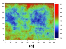
Analysis of reflectance results of silicon wafer samplestexturized by using mechanical grinding reveals that thereflectance over the range of wavelengths studied is alsolowered as a result of grinding only. A considerable change inreflectance is observed with change in the grain size of Al2O3powder (from 8 to 22 lm). The lowering of reflectance may beattributed to increase in average surface roughness parametersRa and Sa and total surface roughness Rt.