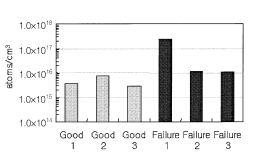
An etching technique for the determination of the metallic impurities distribution in silicon wafers has been developed.An area of 10 mmφ and 10 µm depth was etched by 100 µL of an etching solution with a HF and HNO3 mixture. Theacid matrix was evaporated on the wafer surface by IR lamp illumination and vacuum exhaust. Metallic impuritiesremaining on the wafer surface were redissolved into the collection solution, which was measured by electrothermalatomic absorption spectrometry (ET-AAS). The recovery invested by local etching/ET-AAS was within 95 – 112% forFe, Cu and Ni. The detection limit (3σ) for Fe, Cu and Ni in silicon was 1 × 10¹³ atoms/cm3. To confirm theapplicability, local etching was applied to evaluate the effects of metallic impurities in a gettering study and the electronicproperties of semiconductor devices. It was found that local etching is a useful sample preparation technique for theanalysis of metallic impurities in a specific area on a silicon wafer.
As the packing density increases in an ultra-large-scaleintegrated (ULSI) device manufacturing process, therequirement of an acceptable metallic contamination levelbecomes more stringent.1 Because trace amounts of metallicimpurities affect the performance of electronic devices, a highlyprecise analytical technique is demanded. Vapor-phasedecomposition (VPD) sample preparation is one of the mostprevalent analytical methods for metallic impurity analysis.2,3Oxides on a silicon wafer are decomposed with HF vapor, ormixed acid vapor, and then a liquid droplet is rolled on thehydrophobic surface. VPD preparation has been coupled withseveral different trace elemental analytical techniques, such asinductively coupled plasma mass spectrometry (ICP-MS),4–7atomic absorption spectrometry (AAS)8–11 and total-reflectionX-ray fluorescence (TXRF).
In this paper, the analytical method for a specific area on awafer is described. For the sample preparation of a local areaand a specific depth of a silicon wafer, a sampling apparatus hasbeen developed. The etching area can be easily defined usingthis apparatus at the same fixed positions on several wafers.After preparation, Fe, Cu and Ni were measured by the ETAAS. Determination by ICP-MS or ET-AAS is a commontechnique for the analysis of metallic impurities. Even thoughICP-MS has a lower detection limit, it needs a special sampleintroduction system for a small-volume sample containing Siand HF. Because of a few instrumental limitations, ET-AASwas used in this experiment. As an application using a localetching apparatus, wafers annealed after the contamination ofmetallic impurities and patterned wafers were analyzed.
A wafer was placed between the main plate and the coverplate. A sampling tube was placed in a hole at a specificlocation for the analysis. One hundred microliters of theetching solution were dropped onto the wafer surface encircledby the sampling tube. A vacuum tube was connected in the holeof the sampling tube. The reaction gas was exhausted by avacuum pump, and the etching solution was dried byilluminating an IR lamp under the wafer. After drying etchingsolution, the cover plate and the vacuum tube were removed.Two hundred microliters of a dissolution solution with 1% H2O2and 0.2% HF were pipetted into the sampling tube. Thiscomposition of the dissolution solution was shown to be theoptimum condition to collect metallic impurities on the wafersurface in a previous report.3 The dissolution solution wascollected by a micropipette after one min. The collectedsolution was measured by ET-AAS. All of the experimentswere carried out in a class-100 clean room.

Fig1
It was demonstrated that metallic impurities on a specific areacould be effectively analyzed using a local etching technique.The greatest advantage of the local etching apparatus would beits universal applicability to diverse wafer samples, such aspolished, oxidized and patterned wafers. If the conditions oflocal etching, such as chemical composition or concentration,etching area and etching depth are controlled, the local etchingtechnique could be used to analyze not only the effect ofmetallic impurities on the electronic property of semiconductordevices, but also trace metallic impurities in various devicelayers.