This paper presents a comparative study of the impact of metalwet etch on carrier mobility and metal gate/high-k devicecharacteristics and reliability. A TaSiN metal wet etch process thatis highly selective to the underlying HfO2 dielectric has beendeveloped. While the metal wet etch slightly degraded the electronmobility, it did not affect hole mobility. It did not show any effecton fast transient charge trapping, and, in fact, improved negative biastemperature instability (NBTI) and positive bias temperatureinstability (PBTI). [Keywords: Metal wet etch, High-k, Dual metalgate CMOS, Carrier mobility, Gate dielectric reliability].
As MOSFET dimensions scale into the deep sub-50 nm regime,there is an urgent need to introduce metal gate electrodes and high-kgate dielectrics into CMOS technologies. Replacing poly gateelectrodes with dual metal gates can eliminate poly depletion andavoid problems associated with the poly/high-k gate stack such asboron penetration and Fermi level pinning [1]. A versatile method ofintegrating dual metal gate CMOS is to employ a metal wet etchprocess to selectively remove the first metal from either the NMOSor PMOS region before depositing the second metal [2, 3]. Recently,we have developed metal wet etch processes that are highly selectiveto HfO2 and HfSiON high-k dielectrics and identified SC1 as asuitable wet chemical for several metal gate materials. Using thisselective metal wet etch process, we have successfully fabricateddual metal gate/high-k CMOS transistors with gate lengths down 85nm [4, 5]. The impact of metal wet etch on the time-dependantdielectric breakdown (TDDB) of the HfO2 gate dielectric was foundto be negligible [5]. The effects of HfO2 exposure to wet chemicalHCl on NMOSFET Vt and electron mobility have also been reported[6]. However, detailed studies of the impact of metal deposition plusmetal wet etch on transistor characteristics, especially on devicereliability, are still lacking. In this paper, we present a comparativestudy of the effects of TaSiN metal wet etch on carrier mobility,transient charge trapping, and NBTI and PBTI in TiN/HfO2 CMOStransistors.
Experiments were designed to simulate the impact of metal wetetch on HfO2 gate dielectrics in a dual metal gate CMOS integrationprocess flow [4, 5]. A chemical oxide ~1 nm thick was first grownon a (100) Si substrate. Then 2 nm of HfO2 was deposited byatomic layer deposition (ALD), followed by a NH3 post-depositionanneal. A reactive physical vapor deposition (PVD) process wasused to deposit 10 nm TaSiN, which would serve as the first metalgate in the dual metal gate CMOS flow. TaSiN was then wet etchedusing SC1. In one split, the length of the metal wet etch was targetedto a completely removal of the TaSiN plus a 10% over etch. Inanother split, a much longer over etch time (50%) was used. Theexposed HfO2 was then rinsed in NH4OH to simulate the removal of the α-Si hard mask. Next, 10 nm thick TiN was deposited by ALDtechnique, which would be the second metal in the dual metal gateCMOS flow, capped with a 100 nm α-Si cap. A plasma etch processwas used to etch the gate stack. Other process steps were the same asthose in a conventional poly/SiO2 baseline CMOS flow.
To differentiate the impact of wet chemical exposure from theeffects of metal deposition and metal wet etch, TaSiN metaldeposition was omitted in another experimental split; however, theHfO2 was exposed to SC1 and NH4OH wet chemicals before thedeposition of the ALD TiN metal gate. As a comparison, controlTiN/HfO2 CMOS transistors without the metal deposition and wetchemical exposures were also fabricated.

Fig1
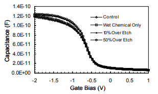
In our previous study, we found that the metal wet etch resulted ina ~0.7 Å effective oxide thickness (EOT) loss in the TaSiN/HfO2stack [4, 5]. Even though this is a small EOT loss, considering thevery high selectivity of SC1 and NH4OH to HfO2 [4, 5], it wasunclear which process step brought about this EOT loss. Figure 1shows the CV characteristics measured on 5X10⁻⁵ cm2 NMOSoverlap capacitors. The EOT is 1.14 nm, 1.12 nm, 1.05 nm, and 10.4nm for the control device, the device that received wet chemicalexposures only, the device that received the 10% over etch, and thedevice that received the 50% over etch, respectively. These resultsconfirm that the SC1 wet etch process itself has very high selectivityto the underlying HfO2. Most of the EOT loss for the device thatreceived the TaSiN wet etch is not incurred by the high-k thickness loss during the metal over etch. Instead, most of the EOT loss (~0.7Å) likely is resulted from the loss of a TaSiN/HfO2 interface layer atthe end of the TaSiN wet etch. The wet etch chemical exposure itselfdid not result in any flat band (Vfb) shift; however, the TaSiNdeposition and wet etch led to a small Vfb shift compared to thecontrol device (from -0.55 V and -0.57 V).
下一篇: 具有宽带隙GaN 半导体的硅上集成光子学