Gallium nitride has been the focus of intense interest inrecent years due to advances in crystal growth technologyand device fabrication procedures. Its direct, wide band gapmakes it an ideal choice for use in various detector applications such as ultraviolet ~UV! astronomy, flame detection,and engine monitoring, where harsh working environmentsexploit the natural durability and visible blindness of thematerial.
Several groups have reported the characterization ofphotoconductive2–5 and photovoltaic positive-intrinsicnegative (p-i-n)6 nitride-based photodetectors. GaNSchottky barrier devices have been shown to have highspeed and low-noise capabilities.7,8 In contrast, much lesswork has been published concerning Schottky-based metal–semiconductor–metal ~MSM! photodetectors. These devicesconsist of two Schottky contacts on a planar surface. GaNMSM detectors with very low dark currents have been demonstrated, but no information about the speed was provided.9In this work, we report the fabrication and characterization ofhigh speed GaN and GaN:Mg MSM photodetectors withsharp wavelength cutoff and high ratio of rejection of visiblelight to UV light.
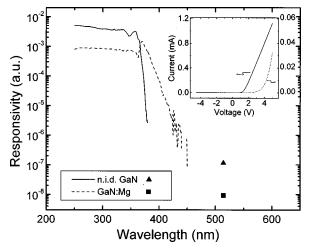
GaN:Mg and nonintentionally doped ~nid! GaN layerswere grown by low-pressure metalorganic chemical vapordeposition on basal plane sapphire. The details of the crystalgrowth have been reported previously.10,11 Low resistivityp-type GaN was achieved in the Mg doped sample after exposure to rapid thermal annealing in a N2 ambient environment. The interdigitated Pt/Au Schottky contacts were deposited by electron-beam evaporation. The fingers were 150mm long and 2 mm wide with a pitch of 10 mm, as seen inFig. 1. In order to study the quality of the Schottky barriers,an indium ohmic contact was deposited near the edge of thesample. The current–voltage (I –V) characteristics measuredbetween the ohmic and Schottky contacts are displayed in the inset of Fig. 2. They show an ideality factor of ;1.5 and;4, for nid GaN and GaN:Mg, respectively, with leakageresistances .10 GV. The dark current value for the GaN:MgMSM detector is ;12 nA at 5 V and is only ;2 nA at 5 Vfor the GaN MSM device, which is additional confirmationof the high quality of the contacts as well as the material.
A Xe arc lamp was used as the optical source for thespectral responsivity studies and a standard synchronous detection scheme was employed to measure the front-side illuminated detector signal. The system was calibrated with anUV-enhanced Si detector. The responsivity dependence onoptical power was determined by excitation with a continuous wave He–Cd laser ~325 nm!. The response time of thedetectors was measured using a pulsed nitrogen laser ~337nm! as the optical source. Noise characterization was performed using a SR760 fast Fourier transform spectrum analyzer with the devices connected to a Keithley 428 currentamplifier, so that the background noise power density of thesystem is about 10224 A2/Hz.
The photocurrent increases linearly with the opticalpower for the GaN:Mg device as seen in Fig. 3, and showsno saturation at higher power levels. The nid GaN device,however, follows a Pk fit, where P is the optical power andk50.9, which is a much better result than the k50.1 behavior reported for nid GaN photoconductors.3 To investigatethe possibility of an internal gain mechanism, the responsiv ity was measured with respect to the voltage bias. The resultsof this test are seen in the inset of Fig. 3. Both the nid GaNand the GaN:Mg MSM devices exhibited a scaling of theresponsivity with voltage bias. This increase indicates thepresence of an internal gain mechanism such as hole trapping. The shape of the spectral response has been found to beindependent of bias up to 5 V.

Fig1
The temporal response of these devices shows no persistent photoconductivity. The dependence of photocurrent response time on load resistance has been analyzed to acquirethe minimum time response of the detector, and is seen inFig. 4. The photocurrent decays are exponential for the nidGaN MSM device. The GaN:Mg device shows exponentialdecays for high load resistances ~.50 kV!, but they becomenonexponential for lower load resistances and tend towards aresponse time of 200 ns, as shown in Fig. 4. In the exponential regimes the time constant is limited by the RC product ofthe system, where R is the load resistance and C is the sum ofthe capacitance of the device and the load capacitance of ourmeasurement system. In order to estimate the minimum timeresponse of the nid GaN MSM detector, the decay time constants are plotted as a function of the load resistance. In orderto find the real speed limitation of the device, these data arefitted to linear functions with zero-load time constants of 10 and 0 ns ~straight and dotted lines in Fig. 4!. From the magnified view of the low load data, shown in the insert, it isclear that this measurement provides the precision only toattest that the time response lies below 10 ns.