Low pressure chemically vapor deposited polysilicon deposition was studied from 525 to 650~ The silicon appears tobe amorphous with a smooth surface up to 550~ and completely crystalline above 600~ The transition region is found tobe from 560 to 590~ This transition is marked by sharp crystallographic and resistivity changes. The smooth surfacemorphology of the amorphous silicon is found to be preserved after POC13 doping and a 1000~ oxidation. The preservationof this smooth morphology is demonstrated to be due to the presence of a native oxide on the surface of the silicon uponexposure to atmosphere. However, an in situ anneal of amorphous silicon at 610~ results in large coarse crystals with roughsurface morphology and disparate orientation. The smooth morphology of the 550~ silicon is found to be transmittedthrough subsequent polycide structure layers. The impact on device reliability is discussed. The amorphous silicon is foundto have a higher plasma etch rate than the polysilicon.
Doped polysilicon is widely used in very large scale integrated (VLSI) device fabrication as gate electrodes, interconnect material, and as resistors in static memory circuits.As gate electrodes, the surface morphology is an importantfactor in device reliability, as the presence of asperities onthe film surface can lead to premature device failures fromlocalized high electric fields. Thus it is highly desirable tohave gate electrodes with smooth surfaces. 1-6 Where devicespeeds of 100 ~s or less are required, the faster access timesrequire even lower resistivity than can be realized withdoped polysilicon. In this instance, therefore, tungsten silicide is often deposited on the doped polysilicon and thepolycide becomes the interconnection material. 6-9 As polycide etching is anisotropic, polycides with rough morphologies require extended overetch to remove highlightresidues. This extended etching may have a propensity forthe pitting of the substrate which would degrade devicereliability. Consequently, polycides with smooth morphologies would be preferred.
The most common technique for silicon deposition is inits crystalline form by tow pressure chemical vapor deposition (LPCVD) from Sill4 at temperatures above 600~ Inthis sequence, in single gas inlet reactors, the depositionrate is such that the silane is depleted down the furnace andthe deposition rate decreases accordingly. To compensatefor this drop in deposition rate, a temperature gradient isoften used, the temperature setpoints being ramped alongthe length of the furnace from the injection points. Thedrop in deposition rate from the silane depletion is, thereby,compensated for by the increase in deposition rate from thehigher temperature. With this approach, while there is uniformity in thickness, the microstructure of the films beinga function of the deposition temperature, would varyacross the reactor. The films would exhibit different properties: optical, morphological, doping, and microstructuraldepending on the location in the reactor. The polysilicondependent device properties may also vary accordingly. Inits crystalline state, polysilicon has a rough surface morphology. However, it is reported that a smooth morphologymay be obtained if the film is deposited amorphously andsubsequently annealed at a higher temperature. 1~Kamins 17 attributed this preservation of the smooth morphology to the presence of a native oxide on the surface ofthe silicon film. Hendricks and Mavero I4 proposed an alternative model. They suggested that the surface smoothnessis preserved because grain growth during annealing involves relatively small atomic distances whereas surfaceroughness requires distances which are large compared tointeratomic distances. The exact mechanism, however, hasnot been established by experimentation. It is, however,important that this mechanism be established.
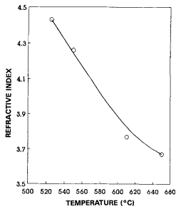
In this study, polysilicon deposition was studied from 525to 650~ primarily to investigate the effect of depositiontemperature on such properties as deposition rate, dopingcharacteristics, surface morphology, etchability, and polycide morphology. The mechanism by which the smooth surface morphology of an amorphous film is preserved afterhigh temperature cycles is also investigated and demonstrated.
A two-step deposition was used to explore the mechanism by which the smooth surface morphology of the amorphous silicon is preserved after a high temperature cycle.The first step was at 550~ for a thickness of 1500 A, andthe second at 610~ for 800 A. One sequence was done insitu and the other was separated with the wafers exposed tothe atmosphere between depositions. Both films werePOCI3 doped and secondary ion mass sepectroscopy(SIMS), TEM, and SEM analyses performed.

Fig1
The degree of the reflection of light from a silicon surfacehas been correlated to the degree of its surface roughness. 12,16 It is reported by Harbeke et al. that at shorter wavelengths (<300 nm), the light penetration depth is less than100 A. 12 Thus is can be assumed that in this wavelengthrange, the incident light probes Sufficiently near the surface that its scatter can be a reflection of the degree of thesurface roughness. In this study, the transmittance at200 nm was measured. Where transmittance is defined asP/Po, P is the radiant power transmitted by the sample andPo is the radiant power incident on the sample. Since thebulk absorption and oxide interface reflection can be ignored in this wavelength range, the transmittance can become a measure of the reflection from the surface. For therest of the document, therefore, this measurement will bereferred to as the reflectivity of the sample. The value forthe reference mirror being 100%, it was assumed that adeviation from that number would reflect the degree oflight scatter and consequently the degree of roughness. Thereflectivity dependence on deposition temperature isshown in Fig. 8 for doped and undoped films.