This paper proposes a new technique to engineer the Fin channel in vertical GaN FinFET toward a straight and smooth channel sidewall. Consequently, the GaN wet etching in theTMAH solution is detailed; we found that the m-GaN plane has lower surface roughness thancrystallographic planes with other orientations, including the a-GaN plane. The grooves and slope(Cuboids) at the channel base are also investigated. The agitation does not assist in Cuboid removalor crystallographic planes etching rate enhancement. Finally, the impact of UV light on m and a-GaNcrystal plane etching rates in TMAH has been studied with and without UV light. Accordingly, it isfound that the m-GaN plane etching rate is enhanced from 0.69 to 1.09 nm/min with UV light; in thecase of a-GaN plane etching, UV light enhances the etching rate from 2.94 to 4.69 nm/min.
As a wide-bandgap transistor technology, GaN provides a compelling opportunityto achieve unprecedented performance levels and efficiency in power electronics systems,owing to its large breakdown electric field and high Baliga’s Figure of merit [1–4]. Itguarantees a 10% reduction of losses in power conversion circuits [5]. Further, it also offersfaster, cooler and smaller power devices than its silicon counterparts.
Thus far, both lateral and vertical structures have been considered to be incorporatedin the GaN power devices [8]. The GaN-based high electron mobility transistor (HEMT)device’s immense potential comes from the high density, the high electron mobility in the2-dimensional electron gas (2DEG) formed at its heterostructure [9]. However, with thehigh electric field close to the device surface, the high current density along the 2D channelgenerates significant heat, increasing the device access resistance and incidences of currentcollapse due to traps [10,11]. Contrariwise, the vertical GaN power devices, especiallythe GaN FinFET, have garnered considerable attention because of their potential to reachhigh voltage and high output current density [12,13]. Furthermore, they exhibit superiorthermal performance compared to lateral devices [14]. The first design and fabricationof a Normally-Off GaN vertical fin power FET (or MOSVFET) have been reported by W.Li et al. [15]. They first used a TCAD tool to investigate the impact of the main critica parameters on the device performance, such as the bulk GaN mobility, the gate-to-gatedistance, and the gate length. They achieved an ON-state resistance (RON) of 2.8 mΩ·cm2and a breakdown voltage (VBR) of 1.2 kV. Several prototype versions of GaN FinFET devicesfabricated on GaN or a foreign substrate have been published in the literature.
The vertical GaN FinFET fabrication process begins with the anisotropic GaN etching,executed by dry Induced Coupled Plasma-Reactive Ion Etching (ICP-RIE) [19]. However,the main drawback of such technology is the GaN sidewall surface’s damage with difficultyin obtaining straight etched sidewalls [20]. Engineering the Fin channel sidewalls plays acrucial role in the electrical performance of vertical GaN FinFET devices [21]. Therefore, itis vital to optimize a smoothing process after dry etching to remove the channel sidewallsimperfections and the GaN/dielectric interface of the device is therefore improved.

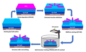
Fig1
For vertical GaN FinFET devices, a Fin channel structure with non-polar plane sidewalls is favorable for Normally-Off operation. Non-polar planes at the FinFET channel’ssidewall are suitable for fabricating the Normally-Off device. Depending on the channelwidth, a low quantity of charge can be present in the channel at VGS = 0 V [22,23]. Them-GaN and a-GaN channel sidewalls revealing process require a specific lithographyorientation of the Fin channel structure [24]. The chemical etching process has also beendemonstrated in the literature for post dry etching treatment of GaN [25–28].To achievethis, Tetramethylammonium hydroxide (TMAH) is widely used [29,30]. Furthermore,UV light-based TMAH etching is also effective technique to enhance the GaN sidewall’setching rate [31]. It also improves the etching selectivity when a dielectric material is usedas a mask.
The purpose of this paper is to investigate one of the most critical steps in the fabrication process of vertical GaN FinFET transistors, which is the etching of the channelsidewalls. An Orientation Determination (OD) technique has also been demonstrated forGaN Fin channel sidewall. Finally, this work presents a procedure to improve the GaNtransistor fabrication process and therefore the performance of the device.
Experiment TechniqueIn this study, we intend to determine the exact orientation of the a-GaN and mGaN planes on the coupon samples, followed by investigating the GaN crystallographicetching with TMAH solution. The GaN channel fingers are firstly fabricated using thetop-down process. The wet etching has been used to reveal the crystallographic planeson the channel sidewalls. The fabrication process has been depicted in Figure 1. A 7 µmthick GaN epi-layer wafer (Sample1) grown by Metal-Organic Chemical Vapor Deposition(MOCVD) on Sapphire substrate is used for this experiment. The size of this square sampleis 1 cm × 1 cm. For this purpose, 180 fingers with 15 × 2 µm2 dimensions oriented from 0◦to 180◦ with a step of 1◦ are fabricated (Figures 1 and 2).