A driving force to achieve increased speed and performance along with higher I/O count is the Flip Chip (FC)Technology which has therefore an high level of importance for a variety of applications. A breakthrough, however,will be the use of flip chip due to cost reduction. For this aim it is essential to use low cost bumping techniques.
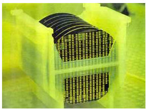
For nearly all existing FC techniques a bumpformation on the chip I/O is needed. Establishedtechniques like the C4 process [1,2] do not fulfill thecost requirements for the consumer market. Aselective chemical plating method can reducebumping cost significantly since it does not requiremasking or metal sputtering. Additionally thistechnique easily allows a parallel processing ofmultiple wafers, leading to a high throughput.The special cost advantage of electroless Ni is givenby the possibility of parallel batch processing. Fig. 1shows a batch of wafers which are processed inparallel. The electroless bumping of 12" wafersallows specific cost savings, especially due to the factthat the 12" equipment for the standard processrequires photo imaging which needs expensivesteppers and 12" sputtering and plating equipment. Incontrast to this the low cost electroless Ni/Aubumping requires special adapted wafer bumpingtanks for the chemical process. This is a special costsaving, because the investment costs are reduced by a factor of 5 -10 compared to a standard electroplatingprocess.
In the FC assembly the Ni/Au bumps fulfill thefollowing function. They protect the Al and act as anadhesion layer and a diffusion barrier and guarantee astable and reliable contact to the Al bondpads [3,4].Besides this, which is mainly the function of a UBM,the Ni can also offer a stand-off, e.g. for chip on glass(COG) using ACF [5]. The feasibility and reliabilityof this bumping process has been proven in a series ofpublished technical papers [3,4,5]. Figure 2 showselectroless Ni/Au as a basis for AnisotropicConductive Adhesive (ACF) Flip Chip Assembly, forpolymeric Flip Chip Assembly (ConductiveAdhesive) and for soldering and direct chip attachtype of applications using different solder alloys.
Electroless Nickel is used in industry for a wide rangeof applications in which Al work pieces are platedwith Ni. The equipment available for these standardprocesses based on large work pieces or printedcircuit boards is not suitable for wafer bumping. Inorder to fulfill the specific requirements for waferbumping a new modular electroless Ni wafer bumpingline has been developed. Each module can takebatches of 50 wafers 8" or 10 wafers 12". Suchprocessing is a key to the extremely high throughputof this bumping line which again determines theoverall cost of the bumping process.

Fig1
Before the wafers can be metallized in the line thewafer backside has to be covered by a stable resistprior to the chemical bumping process. The next stepis a treatment of the pads in an Al cleaner whichremoves oxide layers while the Al surface is microetched. The pretreatment is done in the first modulesof the line. An alkaline zincate solution is used foractivating the Al surface. For the electroless Niplating a bath based on sodium hypophosphite is used.The rate of Ni deposition is 20µm/h. For ahomogeneous Ni deposition on 300 mm wafers acompletely new bumping module was designed andspecial simulations of the Ni flow were done toprevent a minimal tolerance of the Ni heightdistribution on a 12 " wafer. A final Au coating onthe Ni is necessary to prevent oxidation and enableslong-time solderability of bumps. With this Aucoating a maximum Au thickness of 0.25µm can beachieved (typ. 0.05µm). The complete process flow isshown in figure 3. The quality of bumps is controlledby optical microscopy, profilometer measurementsand shear tests. For detailed analysis cross-sectioning,SEM and EDX are used.
下一篇: 使用湿表面处理在抛光氧化铝上进行化学沉积