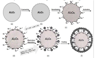
Surface treatment using wet process is very important for the adhesion of metal layers obtained by electrolessdeposition technique. The treatment performed consist of four stages: cleaning, coarsening activation and posactivation. Results showed a good film adhesion of Copper (Cu) and Nickel Phosphorus (Ni-P) by electrolessdeposition. The uniformity of grain structure, its density and the grain size were characterized by scanning electronmicroscopy (SEM). Contact angle was also measured before and after coarsening.
Electroless Deposition (ED) technique is an important metallization method for non-conductive material [1]. It isalso one of the simplest methods for generating thin metallic films on ceramic or polymeric materials compared to othermethods (CVD/PVD, plasma spraying or electrodeposition) [2]. It was found to be very useful for interconnectionapplication on several micro technology assemblies. ED offers high selectivity that allows self-aligned deposition,hence saving lithography steps. ED methods are also very versatile and can produce multi component films. In addition,many metals and alloys can be produced with good quality thin films [3]. Other advantages of ED are: high metalpurity, low operating temperature, planar topography, low cost and applicability for mass production [4]. The purposeof the treatment is to generate nucleation sites for the metals atoms to deposit on. The treatment process before platinginvolves four stages: (i) acid detergent (to remove organic and fingerprint contamination), (ii) coarsening step (to makethe compact and dense surface of ceramics rough, in order to increase the adhesive strength of the deposit metal film tothe ceramic), (iii) activation (Sn, Pd catalyst). In the activation step, the redox reaction takes place between Pd2+ andSn2+ on the substrate where Pd2+ is reduced to Pd0 to catalyse the following ED.[1,5] (iv) Post activation step (to removeexcess of ionic tin from colloid-covered surface, which surrounds the palladium catalyst)[6].
The effect of the treatment is verified by comparing the contact angle before and after the treatment performed onthe ceramic surface. After that, ED of copper and nickel on alumina ceramics was carried out and scanning electronmicroscopy (SEM) was perform to evaluate the morphology of the deposited films.
Electroless deposition onto insulator materials demands the formation of seeds onto the surface so to the depositioncan occur. There are no metallic bonds between the polished alumina and metal coatings but unstable mechanicalcombination [1]. So, acid detergent and coarsening is used to leave the surface free of organic residues and increase themicro roughness of the surface to obtain a hydrophilic surface in order to acquire good adherence for metallic coatingson the surface after nucleation. A widely used procedure for this nucleation involves “sensitization” and “activation” ina stannous chloride and a palladium chloride solution, respectively [8]. Excess tin is usually removed with a solvent forionic tin [6]. Palladium nuclei should then initiate the autocatalytic plating process.
Contact angle images (fig. 2) showed that the surface of the polished alumina prior to the treatment was veryhydrophobic so the drop practically did not spread on the surface, unlike the treated surface, which was quitehydrophilic where the drop greatly spreads.

Fig1
The average grain roughness (Ra) obtained using the software gwyddion v2.47 was 0.094 and 0,082 micronsrespectively for Cu and Ni films and no cracks were observed on the evaluated samples. Both films showed a densestructure and few cavites/holes of very small dimensions after the ED.
As metallic films, in general, do not present good adherence when deposited directly over polished aluminasubstrate, we proposed a surface treatment, as an alternative to other more expensive methods (CVD/PVD, plasmaspraying or electrodeposition.
The four stages treatment process permitted the development of a fully wet Ni and Cu deposition process, being agood alternative to obtain thin high performance flexible films. The surface treatment also showed a high performancein the ED film at low temperature 40 and 30o C for Ni and Cu respectively obtaining more compact metal films and withsmall grain size, when observed through the SEM images.