We have studied selective wet chemical etching of epitaxial GaN layers grown on SiC substrates. Molten KOH and hot orthophosphoric acid were used as etchants. It was shown that due to some features of dissolution of GaN in these etchants, the determination of dislocation density according to the number of etching pits may be erroneous. We have shown that the etching process canbe optimized by introducing Al3+ or Fe3+ ions in hot orthophosphoric acid. As a result, merging of the etching pits was eliminatedand the number of etching pits connected to surface defects on as-grown surface, rather than defects in the bulk of GaN, was minimized. Also, wet etching in hot orthophosphoric acid with Fe3+ and Al3+ ions helped to expose some defects, which might serveas cracking points, in epitaxial GaN layer.
Wet selective chemical etching has been widely used for determination of dislocation density in semiconductors as well as forstudying the character of defect distribution in these materials.Despite the existence of well-established general principles of thisetching, for every particular case the composition of the etchant andoptimal etching conditions should be found empirically, so the etching will give clear etching pits connected strictly to the defects in thematerial.
Gallium nitride is one of the most promising materials for opticaldevices and power electronics, but because of its high chemical stability, wet chemical etching is not yet widely used in postepitaxialtechnology of this material. Only recently, a number of papersshowed a possibility of using wet etching for revealing threading dislocations and micropipes, which characterize epitaxial layers of GaNgrown on foreign substrates, e.g., on sapphire.
In this paper, we report on developing the method of selectiveetching of GaN. Optimum conditions for etching were selected andfactors affecting the character of etching pattern formation werestudied, especially those which might lead to errors in the determination of dislocation density according to the number of etching pits.
The samples used were GaN layers grown on 6H-SiC substratesby HVPE.3 The layers had thicknesses from 2 to 5 µm. Etched samples were studied using standard scanning electron microscopy(SEM) and atomic force microscopy (AFM) techniques. AFM studies were conducted on atomic force microscope SPM-4.
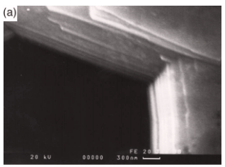
Figure 1 shows a SEM micrograph taken on epitaxial GaN layeretched for 3 min in hot pure H3PO4 (etching in molten KOH gavesimilar results). It can be seen that etching caused the formation ofhexagonally shaped etching pits on the surface of GaN samples.However, those pits did not have smooth walls; rather, the walls hadterraces consisting of planes which were parallel to the basis plane,as is clearly seen in Fig. 2a. These terraces were spreading along thesurface beyond the pit boundaries, causing the pits to merge. Thecharacter of those pits, as far as classical notion of dislocation etching pits is concerned, showed that etching conditions for GaN suggested in Ref. 1 and 2 were not optimal, at least for GaN layersgrown on SiC substrates.

Fig1
It is known that the exposition of defects through etching pits isstrongly affected by the conditions of the surface. If the surfacebefore the selective etching had not been treated with methods, e.g.,electropolishing, which is used for Si before etching it to expose dislocations,8 then etching pits can reflect not only dislocations crossing the surface, but the defect structure of the surface as well. Thatmay also lead to an error when estimating the dislocation densityaccording to the number of etching pits. Unfortunately, the specialtreatment for as-grown surface of GaN is difficult to perform due tothe lack of methods of polishing etching for this material.