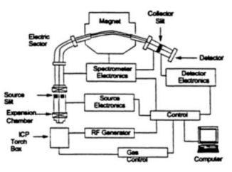
The choice of an adequate analytical technique for contamination control anddefect reduction in the semiconductor manufacturing process is a challengingproblem. Over the past few years, several analytical methods have beenestablished for contamination control. However, given the continuous scaling ofprocess technologies to smaller geometry's, the need to measure even smallerlevels of contamination is becoming important. Sensitivity is not the onlyrequirement; information about possible contaminants is required in the shortestpossible time to prevent manufacturing delays. It is becoming increasinglydifficult for current methods of microcontamination analysis to meet today's needfor sensitivity and high throughput. In this study, several novel methods ofmicrocontamination analysis in chemicals and on silicon surfaces are discussed.The use of magnetic sector ICP-MS as an alterative to the more commonly usedquadrupole ICP-MS for the measurement of chemicals are presented. Betterdetection limits are achieved for many metallic elements without time consumingsample preparation steps. Furthermore, magnetic sector ICP-MS alows theanalysis of P, S, Cl at the ppb detection limit in several chemicals and in DI water. The development of other tools, such as capillary electrophoresis (CE),are discussed. Preliminary results suggest that CE is a cost effective tool for tracemetal analysis in DI water. Sub-ppb detection limits are obtained for 15 elementsin 10 minutes. Surface analysis techniques such as Vapor Phase Dissolution(VPD) are also presented. The strengths and limitations of VPD are discussed inrelation to another method of surface analysis, namely Total Reflectance X-RayFluorescence(TXRF).
As device dimensions are scaled lower in VLSI circuits, the purity of processchemicals and the quality of silicon wafer surfaces are becoming a major concern.Clearly, one requirement for contamination control and defect reduction in the wetprocessing arena is the ability to perform fundamental accurate measurements on theamount of impurities present in high purity DI water and chemicals that are used in thescmiconductor process. The accurate analysis of impurities by suitable analyticaltechniques can then nable more successful measurement of complex time dependentchanges in the process chemistries in the manufacturing environment.
Wafer surface mctallic contamination can be measured by exposing a wafer toHF followed by the extraction of the etched products. This technique is commonlyreferred to as vapor phase dissolution or VPD. By using the magnetic sector highresolution ICP-MS to measure the etched products, high sensitivity surface analysis canalso be performed. Results using this technique will be discussed and compared toalternative methods of analysis such as TXRF.
One of the problems of using an argon ICP as an ion generation source for massspectrometry is that spectral interferences can occur between the analytes of interestwith background molecular peaks, oxide and doubly ionized ions (8-10). Examples ofmajor interferences are listed in Table I. The analysis of typical acids used insemiconductor manufacturing such as HF, NH,OH, HNO, HCl, H,SO can give rise tofurther interferences due to the formation of molecular species as a result of interactionsof argon and oxygen with fluorine, nitrogen chlorine and sulfur (9). Although thcquadrupole mass analyzer is utilized at a resolution sufficient to resolve the massnumber of isotopes across the mass range, this resolution is not sufficient to separate themolecular interferences that nominally exist at the same mass as the analyte metal inquestion. As a result, these molecular interferences can severely limit the ultimatedetection limit that can be obtained.

Fig1
Traditional methods for surface analysis using ion and/or electron beamtechniques have been utilized extensively for surface analysis in the semiconductorindustry. Techniques such as auger electron spectroscopy (AES) (27), secondary ionmass spectrometry (SIMS) (28) have been well characterized. However, as devicedimensions continue to decrease, the need for accurately measuring ultra low levels ofcontamination on surfaces has emerged. It is well known that electron and ion basedspectroscopies are limited to detection limits of 1 x 10' - 1 x 10¹² atoms/cm?.Furthermore, quantification, although possible, is not straightforward with thesetechniques. For example, quantitative auger requires knowledge of factors that correctfor backscattering effects (29,30). As a result of these limitations, significant researchhas been conducted in the semiconductor industry to develop alternative techniques forthe measurement of trace metals. In this section, the vapor phase dissolution (VPD)method will be discussed and compared to Total Reflectance X-RAY Fluorescence(TXRF) techniques.
In VPD techniqucs (31), a bare wafer or an oxidized surface is exposed to HFvapor. After the native or thermal oxide has been removed, a droplet of water is rolledaround the wafer surface to dissolve the metals. In an attempt to improve the collectionefficiency, various types of acidic solutions have been used instead of pure DI water(3l, 32). The droplet is then collected and analyzed by furnace atomic absorptionmethods (24, 31). In order to improve detection limits, quadrupole based ICP-MS havealso been utilized for the analysis of the droplet (14, 32). Figure 9shows thedetection limits of VPD in units of atoms/cm In this experiment, the VPD residue ismeasured using graphite furnace atomic absorption spectroscopy (GFAAS). A VarianA400 GFAAS model was utilized for the experiment Multiple injection methods wereutilized to increase the sensitivity. Figure 10 shows that the detection limits obtainedusing GFAA vary from 5 x10 ' atoms/cm’ to 2 10 atoms/cm’. Despite the highsensitivity obtained, one disadvantage of using a GFAAS is the long time of analysis.With the use of multiple injection technique, the analysis for one element can takeapproximately an hour as compared to about 10 minutes for a normal GFAAS run. Thusthe analysis of a set of elements can take several hours. Moreover, relatively poordetection limits are obtained for the refractory elements such as nickel and titanium.
上一篇: 晶体硅表面金属污染物的化学和物理