A superior control over the surface chemistry of crystalline silicon in wet and dry am-bients is an essential requirement for achieving high product yield in integrated circuitmanufacturing. The continual reduction in feature sizes, necessary to accommodatehigher clock speeds, has emphasized the role of wet wafer cleaning ts meet stringentsurface purity needs. Because of their deleterious effects on device operation, controland detection of trace metals on silicon is especially critical. Meanwhile, increases inprocess complexity have created a need for fast, in situ analysis techniques for earlydetection of process contamination.
Radio frequency photoconductance decay (RFPCD) is a noninvasive techniqueto measure carrier lifetime in silicon. On high bulk lifetime (> 1 ms) silicon, RF.PCD allows the measurement of surface defects with extraordinary sensitivity ( 10cm-2). We have used RFPCD for in situ studies of silicon surface reactions in wetand dry ambients. Ab initio electronic structure calculations at the Hartree-Focklevel were used to model the reactivity of chemisorbed impurities on hydrogen termi.nated silicon. Reasonable agreement was obtained between bond polarity, obtainedfrom population analysis of the electron density results, and experimentally observedreactivity towards polar molecules such as HF and water.
The birth of the modern science of surfaces can be traced to the golden age of germa-nium electronics (1]. After the invention of the point-contact transistor by Shockley,Bardeen and Brattain in 1947, it soon became clear that surface phenomena coulddrastically influence the electrical characteristics of solid state devices. Starting in theearly 1950s, the stabilization of the chemical and electrical properties of germaniumsurfaces became a hot topic in the nascent feld of semiconductor research. Surfacestates, proposed earlier on theoretical grounds by Tamm (2] and Shockley (3], werefirst used by Bardeen in 1947 (4] to explain the observed discrepancy between metalwork functions and the barrier heigths at metal/semiconductor contacts. The sameconcept later entered semiconductor textbooks as a convenient link between electricaland chemical processes at the semiconductor surface. In all of the early germaniumwork, poor crystal quality tended to compromise reproducibility, and lack of sensitivesurface analysis tools led to limited understanding of the reaction chemistry. Never-theless, the foundations were laid for a new feld of materials research: semiconductorsurface science.
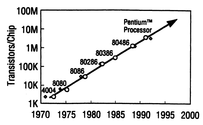
Today's most advanced microprocessors contain millions of devices (mostly MOSFETs) with features as small as 0.35 pm, and run at clock speeds greater than 250MHz. The phenomenal progress in integrated circuit (IC) performance during thelast three decades is due to a famous industry paradigm. Moore's Law (5], whichpredicts the doubling of the number of devices per chip every 18 months (Figure 1.1)The migration towards smaller features and larger die sizes confronts the IC industry with some formidable technical and financial challenges, arising from the need tocontinuously lower defect densities on substrates with increasing diameter.

Fig1
It has been projected that metallic surface contamination levels will have to besuppressed below 10°atoms/cm2 to obtain satisfactory device yield for future ULSI(Ultra Large Scale Integration)(7]. Concurrently, a tight control over particulate con-tamination will continue to grow more important with each subsequent IC generationas the size of a “killer particle in photolithography scales with minimum featuresize. As cleanliness standards continue to grow tighter, chemisorption of gaseous con-taminants from the cleanroom ambient onto the wafer surface is causing increasingconcerns as well. Oxygen chemisorption is known to degrade thin film quality in epilayer growth and metallisation processes (12], while chemisorbed organics may severlydegrade GOl and epilayer quality (13]. For thin gate oxides (<100 A), atomic scaleincreases in surface roughness, have been shown to affect GOI also.
上一篇: 铜污染对薄栅氧化层完整性的影响
下一篇: 过程化学品和去离子水以及硅表面