Contamination of silicon with trace amounts of copper during processing can adversely affect the gate oxide integrity of integrated circuits, resulting in substantial yield loss and reliability problems. Because of increased use of copper as interconnect material, cross-contamination during the production process must be avoided. Establishing adequate protocols for wafer handling and tool use requires understanding of the mechanisms by which copper affects the gate oxide and knowledge of acceptable contamination limits. The effect of copper contamination on thin gate oxide integrity was studied by purposely introducing small amounts of copper in controlled contamination experiments.
Copper contamination causes gate oxide defects by precipitating near the Si/SiOi interface when the silicon is cooled from the processing temperature. The concentration at which defects start to appear on flat capacitors decreases with decreasing oxide thickness. When copper contamination from a contaminated ammonium hydroxide peroxide mixture cleaning solution occurs, deposition of more than 7 x 10'° atoms/cm" is required before the gate oxide integrity of 3 nm oxides is affected. Such levels are not readily exceeded in state of the art integrated circuit fabrication facilities using highgrade chemicals.
Copper deposition from contaminated hydrofluoric acid (HF) solutions results in oxide lifetime degradation for 3 nm oxides even when less than 1 x 10'° atoms/cm" is deposited. The copper catalyzes hydrogen evolution, which in turn causes dissolution.and thus roughening, of the silicon surface. Roughening of the silicon is responsible for the reduced oxide quality. Thus, removal of the copper after contamination has occurred does not lead to recovery of the oxide quality. A copper contaminated silicon surface, which is immersed in uncontaminated HF, will also have reduced oxide lifetime.
Present semiconductor processing is donunated by Complementary Metal Oxide Semiconductor (CMOS) technology. In a Metal Oxide Semiconductor Field Effect Transistor (MOSFET), a gate dielectric is used to electrically insulate the gate from the channel region while still allowing control of that channel through its capacitance. Thermally grown silicon dioxide has traditionally been used as gate dielectric because of its excellent electrical and chemical properties (wide bandgap, high breakdown field, high thermodynamic stability and excellent interface with monocrystalline silicon).
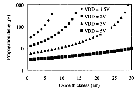
Scaling the MOSrcT to smaller channel lengths requires that the gate capacitance be increased (see section 1.1 for the reasons). Silicon dioxide's relative dielectric constant of only 3.9 means that extremely thin layers are required to achieve the desired capacitance. Oxide thickness is expected to scale linearly with the channel length by the authors of the National Technology Roadmap for Semiconductors (Table l.l). Industry representatives generally indicate that more aggressive scaling will be required.
The drastic reduction in oxide thickness results in manufacturing and fundamental difficulties. Uniformity and reproducibility requirements become more difficult to meet. Boron penetration of the oxide becomes an issue. Yield targets become harder to meet and reliability of thin oxides is not well understood. Ultimately, the required oxide thickness (from a capacitance point of view) will become too small to restrict current flow between the gate and the chaimel of the MOSFET. However, because silicon dioxide has proved its use over the years, because it is easy and cheap to grow on a silicon wafer and because is a well understood material, it is likely to remain in use as gate dielectric as long as possible. Change to an alternate gate dielectric is risky and is likely to be expensive. Therefore, identifying and resolving (where possible) the problems very thin oxides face in use as a gate dielectric is of great importance to the microelectronics industry.

Fig1
Direct tunneling occurs when the oxide voltage is smaller than the barrier height while Fowler-Nordheim tunneling occurs when larger oxide voltages are present. Figure 1.2 shows measured tunnel current curves for some thin oxides. The change in slope indicates the change in tunneling mechanism.
A fit of analytic current-voltage relationships with measured data shows a good fit for voltages above 1.5 V [7]. The analytic direct tunneling current equation results does not fit the measured direct tunnel current well for low voltages because the condition of degenerate accumulation is not satisfied for low voltages. The calculated current can be several orders of magnitude too large. A more careful approach which treats the inversion or accumulation layer as a narrow potential well and solves the complete Schrodinger equation results in a much better fit to measured data [8]. Unfortunately this solution can not be expressed analytically. This quantum mechanical correction also has been shown to explain deviations in the capacitor-voltage characteristics for very thin oxides [8]. The effect of the quantum mechanical corrections is to shift the inversion or accumulation charge away from the interface model (resulting in an apparent increase in oxide thickness). The corrections therefore predict a reduction in tunnel current versus the analytical model. These effects are the result of the large value of the gate capacitance and are therefore not limited to an SiOi gate dielectric. Treatment of high-K dielectric materials must deal with these issues too. For very thin oxides, it is essential that polysilicon depletion, degenerate carrier statistics and confinement effects be considered simultaneously for accurate simulation of the MOS structure, particularly at low gate voltages.
下一篇: 晶体硅表面金属污染物的化学和物理