Surface texturing is one of the methods that improve the conversion efficiency of silicon-based solarcells by increasing the light trapping. The anisotropic texturing of p-type silicon (100) surface wasperformed using alkaline etching solution of sodium hydroxide (NaOH) including isopropyl alcohol(IPA) and hydrazine hydrate. The optical properties of etched wafers were investigated usingreflectance spectrometer and morphology of surface was studied using scanning electron microscopy(SEM). Influence of NaOH concentration on etched wafers was studied and optimum value of surfacereflectance was obtained by applying the best concentration of alkaline solution (NaOH).
Surface texturing of silicon wafer is a widely usedprocess in various applications such as solar cellindustry and detector applications. The most suggestedetchants are sodium hydroxide (NaOH) and potassiumhydroxide (KOH) [1]. In 1967, Price used chemicaletching of silicon for the first time [2]. His etchingsolution was composed of potassium hydroxide (KOH),water (H2O) and isopropyl alcohol (IPA). In 1969, Leedeveloped this method by applying hydrazine hydrate(N2H4) in the etching solution [3]. Hydrazine played therole of oxidant and IPA was a complex agent. In thisstudy, silicon texturing was investigated by applyingalkaline anisotropic etching solution consisting ofsodium hydroxide (NaOH), isopropyl alcohol (IPA),and hydrazine hydrate. The advantage of alkalineanisotropic etching solution is homogeneous etching ofSi (100) substrates. In this report, we have optimizedtexturing of silicon for trapping the incident light inorder to reduce light reflection from silicon surfaces.This technique was used in thin film solar cells toachieve a higher efficiency. The etching process leads tothe formation of pyramidal structures with planeorientation of {111} on surface of substrate.Fig. 1 schematically shows the formation of pyramidalstructures.
A high-doped p-type silicon (100) wafer with resistivityin range of 1-35 Ωcm was used as the substrate. Theexperiments were performed on square samples (20 mm× 20 mm) with a thickness of 250 µm. before etching,silicon surface was chemically cleaned using aconventional RCA method to remove the particulatematters on the surface [4]. Adopting the method, thesubstrates were successively dipped in 1:1:5 (byvolume) of NH4OH:H2O2:H2O for 10 min, 1:50 (byvolume) of HF:H2O for 20 s, and then in 1:1:6 (byvolume) of HCl: H2O2: H2O for another 10 min. Thesamples were then washed with deionized water (DI).
During the texturing process of silicon, hydroxyl ions(OH-) are bonded to two Si dangling bonds. The Si-OHbond makes the two silicon back bonds weak.Therefore, the silicon hydroxide complex is formed.After this process, the monosilicic acid is formed. Thefour electrons in the silicon conduction band aretransferred to four water molecules.

Fig1
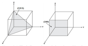
The morphology of etched surface is dependent onseveral parameters such as temperature, concentrationsolution, etching time, atomic defects andcrystallographic orientation of Si wafers. One of themost important parameters is the positions of atoms inSi lattice. Fig. 2 shows different crystal planes of Sidescribed by Miller indices. The density of Si atomswhich are in (111) plane is higher than that in (100)plane, therefore (100) planes can be easily dissolved inetchants but (111) planes are more resistive to theetchants and the etch rates of these planes are slower.Therefore, micro-pyramids of silicon are formed byanisotropic etching of silicon wafer with (100) crystalorientation [5-6].
Silicon micro-pyramidal textures were fabricated bychemical etching process in order to reduce thereflectance spectra of crystalline silicon surface invisible range. The Si pyramids with high uniformity canprovide high antireflection properties. Therefore, it canpromise potential applications in highly efficient,silicon-based solar cells. In this report, formation of Simicro-pyramidal structures was optimized by applyingdifferent concentration of NaOH in etching solution.