GaN-based light emitting diodes (LEDs) have received much attention in recent years as high-brightness light sources.1 Sapphiresubstrates account for approximately 85% of all substrate materialsused in the manufacture of LEDs. Nevertheless, the large contrast inrefractive index between sapphire (n = 1.7), GaN (n = 2.4) and air(n = 1), may cause low light extraction efficiency (LEE) because ofthe undesired total internal reflection at the interface between the chipand air. GaN epitaxial films directly grown on flat sapphire substratesalso contain a high density of threading dislocations (TDs) (typically>1010 cm−2) owing to lattice mismatch between GaN and sapphire.2TDs act as electron leakage paths and nonradiative recombinationcenters in multiple quantum wells, thus degrading internal quantumefficiency (IQE) and shortening lifetime of LEDs.3 Intensive studieshave been carried out to improve LEE, IQE and lifetime of GaN-basedLEDs.
Patterned sapphire substrates (PSS), i.e., etched sapphire substrateswith periodically patterned artificial structures, have been found to beeffective in improving the performance of GaN-based LEDs.4,5 Theunderlying mechanism is that PSS, compared to flat substrates, contribute to the higher IQE and LEE through two beneficial effects. First,the sidewalls of patterns change the scattering directions of lights, thussubstantially suppressing the undesired total internal reflection at theGaN/sapphire and GaN/air interfaces.6 It has been proposed that theslant angle of PSS patterns is a critical factor in affecting the LEEof LEDs.7 The simulation indicated that pyramid arrays with a slantangle of 25◦–60◦ effectively increased the LEE, and the illumination intensity was highest at a specific slant angle of ∼33◦.8 Second,presence of patterns considerably reduces the density of TDs in GaNlayers owing to the bend of dislocations between the trench region ofpatterns during the epitaxial growth.9 It was reported that the densityof TDs in the GaN layer could be reduced significantly by three orders of magnitude (from 1010 cm−2 to 107 cm−2) using the cone-shapedPSS (CPSS).
The geometric shape of PSS affects the crystal quality of GaN epitaxial layer and the LEE of LEDs.11–13 Patterns with various geometricshapes, including grooves,14 circular concaves,15 cones,10 pyramids,16volcanos17 or hemispheroids,18 have been created by either dry or wetetching methods. By dry etching — usually plasma etching, only patterns with simple geometries of cones, cylinders, hemispheroids canbe fabricated. On the contrary, wet etching enables crystallographicspecific etching so that more sophisticated patterns such as pyramidswith multiple crystallographic planes can be fabricated using etchantslike mixture of H2SO4 and H3PO4 at elevated temperature.
Because wet etching enables more sophisticated crystallographicspecific etching of PSS samples by varying temperature and/or themixture ratio of H2SO4 to H3PO4, efforts have been devoted to createvarious crystallographic planes, and to further study the evolution ofexposed crystallographic planes.21,22 Under different wet etching conditions, crystallographic planes of low Miller index like R-plane,14,23N-, M-, A-planes24–26 and other planes of higher Miller index20,27have been reported. Recently, a two-step wet etching study (H3PO4-based etchants without detailed information given about constituentsand compositions, 270◦C) was carried out to investigate the formation of crystallographic planes of pyramid PSS.22 The evolution ofcrystallographic planes of CPSS under the wet etching condition(H2SO4:H3PO4 = 3:1 at volume ratio, 230◦C) was reported.19 However, there are two issues yet to be satisfactorily addressed. First,present investigations about the evolution of crystallographic planesleave much room for systematic studies, i.e., full range of etching conditions needs to be covered, and careful comparisons between differentstarting pattern shapes of PSS (e.g., cylinders versus cones) are alsoneeded to elucidate the etching mechanism. Second, the significanceof accurate and comprehensive topography characterizations of PSShas not been fully recognized for correct determination of dimensions,Miller indexes, as well as etching rates of exposed crystallographicplanes.

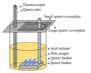
Fig1
The etching process was quasi-continuous. The quartz basketloaded with up to 12 samples was placed on the inner bottom ofthe beaker as the mixture temperature reached 230◦C and remainedstable. When a specific time was reached, the smaller rectangular coverplate was uncovered, the basket loaded with samples was quickly(within 5 s) removed from the etchant. A piece of sample was removed from the groove of basket by a pair of tweezers and droppedinto ultrapure water (18.2 M/cm) in a clean polyfluortetraethylene(PTFE) plasticware. Then the basket was immediately placed backinside the beaker, the smaller coverplate was placed back to recoverthe rectangular opening in the large coverplate. The steps above wererepeated for other samples. Presumably because the volume of basketwas quite small compared to the volume of etchant and the handlingoperation was rather swift, we did not observe significant temperature fluctuations during the sampling progress. The etching experiments were repeated more than one to check the reproducibility of theresults.
上一篇: GaN薄膜的光学图案化